
InP의 웨이퍼
PAM-XIAMEN은 낮은 도핑, N 유형 또는 반절연을 포함한 프라임 또는 테스트 등급의 VGF InP(인화인듐) 웨이퍼를 제공합니다. InP 웨이퍼의 이동도는 유형에 따라 다릅니다. 저도핑 웨이퍼>=3000cm2/Vs, N 유형>1000 또는 2000cm2V.s(도핑 농도에 따라 다름), P 유형: 60+/-10 또는 80+/-10cm2 /Vs(다른 Zn 도핑 농도에 따라 다름) 및 반모욕적인 경우>2000cm2/Vs인 경우, 인화인듐의 EPD는 일반적으로 500/cm2 미만입니다.
- 기술
제품 설명
InP의 웨이퍼
PAM-XIAMEN, a leading InP wafer supplier, offers Compound Semiconductor InP wafer – Indium Phosphide which are grown by LEC(Liquid Encapsulated Czochralski) or VGF(Vertical Gradient Freeze) as epi-ready or mechanical grade with n type, p type or semi-insulating. The InP wafer orientation (111) or (100) is available. And the dopants can be Sulphur, Sn(Tin), Zinc or customs. The Laser Mark as specified on backside of InP wafer along with primary flat. The orientation with slight deflection angle is available, such as (100)0.075° towards [110]]±0.025°.
Indium phosphide (InP) is a binary semiconductor composed of indium and phosphorus. It has a face-centered cubic (“zinc blende”) crystal structure, identical to that of GaAs and most of the III-V semiconductors. Indium phosphide can be prepared from the reaction of white phosphorus and indium iodide [clarification needed] at 400 °C., also by direct combination of the purified elements at high temperature and pressure, or by thermal decomposition of a mixture of a trialkyl indium compound and phosphide. Indium phosphide wafers are used in high-power and high-frequency electronics [citation needed] because of the superior electron velocity with respect to the more common semiconductors silicon and gallium arsenide. The InP wafer size we can offer is 2”, 3” and 4”, and the InP wafer thickness will be 350~625um.
다음은 세부 사양은 다음과 같습니다
| Specifications | ||||
| Dopant | N-type | N-type | P-type | SI-type |
| Conduction Type | low doped | Sulphur | Zinc | lron |
| Wafer Diameter | 2″ | |||
| Wafer Orientation | (100)±0.5° | |||
| Wafer Thickness | Min:325 Max:375 | |||
| Primary Flat Length | 16±2mm | |||
| Secondary Flat Length | 8±1mm | |||
| Carrier Concentration | 3×1016cm-3 | (0.8-6)x1018cm-3 | (0.6-6)x1018cm-3 | N/A |
| Mobility | (3.5-4)x103cm2/V.s | (1.5-3.5)x103cm2/V.s | 50-70×103cm2/V.s | >1000cm2/V.s |
| Resistivity | N/A | N/A | N/A | N/A |
| EPD | <1000cm-2 | <500cm-2 | <1×103cm-2 | <5×103cm-2 |
| TTV | <10um | |||
| BOW | <10um | |||
| WARP | <12um | |||
| Laser marking | upon request | |||
| Suface finish | P/E, P/P | |||
| Epi ready | yes | |||
| Package | Single wafer container or cassette | |||
2″ P Type InP Wafer Specification
| 매개 변수 | UOM | |
| 자료 | InP를 | |
| Conduct Type/Dopant | S-C-P/Zn | |
| Grade | Prime | |
| Diameter: | 50.5±0.4 | mm |
| Orientation: | (100)±0.5° | |
| Orientation Angle: | / | |
| Thickness: | Min:325 Max:375 | um |
| Carrier Concentration: | Min:0.6E18 Max:3E18 | cm-3 |
| Resistivity: | Min:/ Max:/ | ohm.cm |
| Mobility: | Min:/ Max:/ | cm-2/V.sec |
| EPD: | Ave<:1000 Max<:/ | cm-2 |
| TTV: | Max:10 | um |
| TIR: | Max:10 | um |
| BOW: | Max:10 | um |
| Warp: | Max:15 | um |
| Flat Option: | EJ | |
| Primary Flat Orientation: | (0-1-1) | |
| Primary Flat Length: | 16±1 | mm |
| Secondary Flat Orientation: | (0-11) | |
| Secondary Flat Length: | 7±1 | mm |
| Suface: | Side 1:Polished Side 2:etched | |
| Edge Rounding | 0.25(Conform to SEMI Standards) | mmR |
| Particle Count: | / | |
| Package | individual container filled with N2 | |
| Epi-ready | Yes | |
| Laser Marking | Back side major flat | |
| Remark: | Special specifications will be discussed separately | |
3″ InP Wafer Specification
| Specifications | ||||
| Dopant | N-type | N-type | P-type | SI-type |
| Conduction Type | 저농도 도핑 | Sulphur | Zinc | lron |
| Wafer Diameter | 3″ | |||
| Wafer Orientation | (100)±0.5° | |||
| Wafer Thickness | 600±25um | |||
| Primary Flat Length | 16±2mm | |||
| Secondary Flat Length | 8±1mm | |||
| Carrier Concentration | ≤3×1016cm-3 | (0.8-6)x1018cm-3 | (0.6-6)x1018cm-3 | N/A |
| Mobility | (3.5-4)x103cm2/V.s | (1.5-3.5)x103cm2/V.s | 50-70×103cm2/V.s | >1000cm2/V.s |
| Resistivity | N/A | N/A | N/A | N/A |
| EPD | <1000cm-2 | <500cm-2 | <1×103cm-2 | <5×103cm-2 |
| TTV | <12um | |||
| BOW | <12um | |||
| WARP | <15um | |||
| Laser marking | upon request | |||
| Suface finish | P/E, P/P | |||
| Epi ready | yes | |||
| Package | Single wafer container or cassette | |||
4″ InP Wafer Specification
| Specifications | ||||
| Dopant | N-type | N-type | P-type | SI-type |
| Conduction Type | low doped | Sulphur | Zinc | lron |
| Wafer Diameter | 4″ | |||
| Wafer Orientation | (100)±0.5° | |||
| Wafer Thickness | 600±25um | |||
| Primary Flat Length | 16±2mm | |||
| Secondary Flat Length | 8±1mm | |||
| Carrier Concentration | ≤3×1016cm-3 | (0.8-6)x1018cm-3 | (0.6-6)x1018cm-3 | N/A |
| Mobility | (3.5-4)x103cm2/V.s | (1.5-3.5)x103cm2/V.s | 50-70×103cm2/V.s | >1000cm2/V.s |
| Resistivity | N/A | N/A | N/A | N/A |
| EPD | <1000cm-2 | <500cm-2 | <1×103cm-2 | <5×103cm-2 |
| TTV | <15um | |||
| BOW | <15um | |||
| WARP | <15um | |||
| Laser marking | upon request | |||
| Suface finish | P/E, P/P | |||
| Epi ready | yes | |||
| Package | Single wafer container or cassette | |||
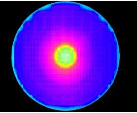
PL(Photoluminescence) Test of 인듐 인화물 Wafer
We measure InP wafers by Peak Lambda, Peak int, and FWHM, the spectra mapping is as follows:

About InP Wafer Application
As a new type of compound semiconductor material, InP wafer market share is increasing gradually. Due to the excellent indium phosphide properties, the performance of microwave power source devices, microwave amplifiers and gate FETs fabricated on InP material will be better than those fabricated on existing gallium arsenide materials. Indium phosphide heterojunction lasers are also extremely promising light sources in optical fiber communications.
InP wafer fabrication for devices, like growing millimeter wave microelectronic devices and optoelectronic device materials for optical fiber communications, is widely used. With the continuous improvement of device performance and the reduction of device size, the quality requirements for indium phosphide wafers are getting higher and higher. Therefore, the InP wafer process is optimizing gradually.
The the typical values is see below data:
| Peak Lambda(nm) | Peak Int | FWHM(nm) |
| 1279.4 | 7.799 | 48.5 |
| 1279.8 | 5.236 | 44.6 |
당신은 또한 같은 수 있습니다 ...
-
갈륨 비소 (갈륨 비소) 웨이퍼
선도적인 GaAs 기판 공급업체인 PAM-XIAMEN은 프라임 등급 및 더미 등급의 반도체 n형, 반도체 C 도핑 및 p형을 포함한 Epi-ready GaAs(갈륨 비소) 웨이퍼 기판을 제조합니다. GaAs 기판 저항률은 도펀트에 따라 달라지며, Si 도핑 또는 Zn 도핑은 (0.001~0.009) ohm.cm이고, C 도핑은 >=1E7 ohm.cm입니다. GaAs 웨이퍼 결정 방향은 (100)과 (111)이어야 합니다. (100) 방향의 경우 2°/6°/15° 어긋날 수 있습니다. GaAs 웨이퍼의 EPD는 일반적으로 LED의 경우 <5000/cm2이고 LD 또는 마이크로 전자공학의 경우 <500/cm2입니다.
-
GaSb 및 웨이퍼
PAM-XIAMEN은 LEC(Liquid Encapsulated Czochralski)에 의해 성장된 n형, p형 또는 반절연의 다른 방향(111) 또는 (100)을 갖춘 epi-ready 또는 기계적 등급으로 성장한 화합물 반도체 GaSb 웨이퍼(갈륨 안티모나이드)를 제공합니다.
-
SiC를 에피 택시
우리는 실리콘 카바이드 장치의 개발 6H 또는 4H 기판 상에 정의 박막 (탄화 규소)의 SiC 에피 택시를 제공한다. SiC를 에피 웨이퍼는 주로 쇼트 키 다이오드, 금속 산화물 반도체 전계 효과 트랜지스터, 접합 전계 효과에 사용 -
의 InAs 웨이퍼
PAM-XIAMEN은 LEC(Liquid Encapsulated Czochralski)에 의해 성장된 인듐 비소 웨이퍼인 화합물 반도체 InAs 웨이퍼를 n형, p형 또는 다른 방향(111) 또는 (100)의 반절연을 갖춘 Epi-Ready 또는 기계적 등급으로 제공합니다. 또한 InAs 단결정은 전자 이동도가 높아 홀 장치를 만드는데 이상적인 재료입니다.
-
GaP 웨이퍼 – 일시적으로 제공할 수 없음
PAM-XIAMEN은 LEC(Liquid Encapsulated Czochralski)에 의해 성장된 인화갈륨 웨이퍼인 화합물 반도체 GaP 웨이퍼를 n 유형, p 유형 또는 다른 방향(111) 또는(100)의 반절연을 갖춘 에피 준비 또는 기계적 등급으로 제공합니다. -
창 (게르마늄) 싱글 수정 및 웨이퍼
PAM-XIAMEN은 2", 3", 4" 및 6" 게르마늄 웨이퍼를 제공합니다. 이는 VGF/LEC에서 성장한 Ge 웨이퍼의 약자입니다. 가볍게 도핑된 P 및 N 유형 게르마늄 웨이퍼는 홀 효과 실험에도 사용할 수 있습니다. 실온에서 결정질 게르마늄은 부서지기 쉽고 가소성이 거의 없습니다. 게르마늄은 반도체 특성을 가지고 있습니다. 고순도 게르마늄에 3가 원소(예: 인듐, 갈륨, 붕소)를 도핑하여 P형 게르마늄 반도체를 얻습니다. 및 5가 원소(안티몬, 비소, 인 등)를 도핑하여 N형 게르마늄 반도체를 얻습니다. 게르마늄은 높은 전자 이동성과 높은 정공 이동성과 같은 우수한 반도체 특성을 가지고 있습니다. -
InSb를 웨이퍼
PAM-XIAMEN은 화합물 반도체 InSb 웨이퍼 - LEC(Liquid Encapsulated Czochralski)에 의해 n 유형, p 유형 또는 다른 방향(111) 또는 (100)의 반절연을 갖춘 Epi-Ready 또는 기계적 등급으로 성장한 안티몬화 인듐 웨이퍼를 제공합니다. 등전자로 도핑된 안티몬화인듐(예: N 도핑)은 안티몬화인듐 박막 제조 공정 중 결함 밀도를 줄일 수 있습니다.
-
프리 스탠딩 GaN 기판
PAM-XIAMEN는 UHB-LED 및 LD위한 (질화 갈륨), GaN 기판 웨이퍼를 자립의 제조 기술을 확립했다. 수 소화물 기상 성장 (HVPE) 기술에 의해 성장 우리 GaN 기판은 낮은 결함 밀도를 갖는다.