PAM-XIAMEN Offers GaAs LED epitaxy wafer, which is AlGaInP LED (Red LED) stack on GaAs substrate. Xiamen Powerway Advanced Material Co.,Ltd., a leading supplier of 갈륨 비소 epi wafer 및 기타 관련 제품과 서비스의 크기는 2 "& 4"의 새로운 출시를 발표했다이 새로운 제품은 PAM-하문의 제품 라인을 자연스럽게 추가를 대표하는 2010 년에 대량 생산에 있습니다.
Dr. Shaka, said, “We are pleased to offer GaAs LED epi wafer to our customers including many who are developing better and more reliable for Red Led. It includes AlGaInP led structure with multi quantum well, including DBR layer for LED chip industry, wavelength range from 620nm to 780nm by MOCVD. Therein, AlGaInP is used in manufacture of light-emitting diodes of high-brightness red, orange, green, and yellow color, to form the heterostructure emitting light. It is also used to make diode lasers.The availability improve boule growth and wafering processes.” and “Our customers can now benefit from the increased device yield expected when developing advanced transistors on a square substrate. Our led epitaxy on GaAs substrate are natural by products of our ongoing efforts, currently we are devoted to continuously develop more reliable products.”
PAM-XIAMEN’s improved AlGaInP led structure product line has benefited from strong tech support from Native University and Laboratory Center.
1. 610~630nm Red LED Reverse Polarity Structure
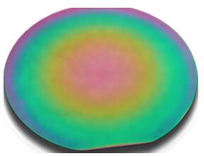
No.1 GaAs LED Wafer for Red Light
| Layer | 자료 | Thickness (nm) |
| p-contact | GaP: C | 104 |
| p-window | GaP: Mg | – |
| p-spreading | AlGaInP: Mg | – |
| p-cladding | AlInP: Mg | 297 |
| Spacer | AlInP | – |
| Active region | AlGaInP | – |
| n-cladding | AlInP: Si | – |
| n-spreading | Al0.6GaInP: Si | – |
| ? | InGaP: Si | – |
| n-contact | GaAs: Si | 80 |
| Etch stop layer | InGaP: Si | – |
| 완충기 | GaAs: Si | – |
| 기판 | GaAs: Si | 350000 |
No.2 GaAs Red LED Epitaxy Wafer
| 구조 | Thickness(nm) |
| C-GaP | 104 |
| Mg-GaP | – |
| Mg-AlGaInP layer | 42 |
| Mg-AlInP | – |
| AlInP | 63 |
| MQW,AlGaInP | – |
| Si-Al0.6GaInP | 296 |
| Si-GaInP | – |
| Si-GaAs | 8.8 |
| Si-GaInP | – |
| Si-GaAs buffer | – |
| GaAs 기판 | 230 |
Electro-optical Characteristics(Lf–=20 mA, 22℃)
| Model name | WD Code | WLD(λd, nm) | VF(Vf, V) | Reverse current(Ir, μA) Vr=-10V |
| PL065RL | 630D | 630-635 | 1.90-2.20 | 0-1 |
| 635D | 635-640 | |||
| 640D | 640-645 |
| Electro-optical Characteristics (@20deg. 20ma) | ||||
| Item No. | WLD(nm) | VF(V) | IR(uA)@Vr=-10 | IV |
| PAM630U | 630-640 | 1.8<Vf<2.2 | 0<IR<1 | 25-38 |
Radiant Flux(Lf–=20 mA, 22℃)
| Radiant Flux(LOP, mcd) | |||||||||||
| Code | LU | LV | LW | LX | LY | LZ | LO | L1 | L2 | L3 | L4 |
| LOP(mcd) | 20-25 | 21-26 | 22-27 | 23-28 | 24-29 | 25-30 | 26-31 | 27-32 | 28-33 | 29-34 | 30-35 |
Above are reverse polarity structures, and we also can supply positive structure of GaAs LED wafer, detailed structure please consult us at victorchan@powerwaywafer.com.
The difference between the reverse polarity red light and the positive red light of LED is that the positive pole of the red chip is below and the negative electrode is on above. Therefore, the structure of positive LED wafer and reverse polarity LED wafer is different.
After the LED epitaxy wafer manufacturing process, the epitaxial wafer of GaAs-based LED is made in chip, the traditional red and yellow LED chips are soldered on the bracket with the positive electrode facing up and the negative electrode down. Later developed red and yellow LED chips have the negative electrode upward, and the positive electrode is installed in the reverse traditional direction on the bracket, which is called reverse polarity chip. The material and process of red and yellow reverse polarity LED chips are different from those of traditional red and yellow LED chips. The luminous efficiency of reverse polarity LED chips is higher than that of traditional polarity LED chips. Now the reverse polarity chip has become the mainstream of red and yellow LED chips.
In addition to the difference in luminous efficiency, the use method and specification of installed lamp beads are the same.
2. About GaAs Material
갈륨 비소는 마이크로파 주파수 집적 회로, 모 놀리 식 마이크로파 집적 회로, 적외선 발광 다이오드, 레이저 다이오드, 태양 전지, 광 윈도우와 같은 디바이스의 제조에 사용된다.
GaAs로 종종 인듐 갈륨 비소, 알루미늄 갈륨 비소 등을 포함하는 다른 III-V 반도체의 에피 택셜 성장 용 기판의 재료로서 사용된다.
갈륨 비소의 일부 전자 성질은 실리콘보다 우수하다. 이것은 갈륨 비소 트랜지스터 250 개 헤르쯔 초과하는 주파수에서 작동 할 수 있도록 높은 포화 전자 속도와 높은 전자 이동도를 갖는다. 갈륨 비소 장치는 넓은 밴드 갭 에너지에 의해 과열에 비교적 둔감하고 또한, 특히 고주파수에서, 실리콘보다 전자 회로 장치에서 (전기 신호에 잡음) 적은 노이즈를 생성하는 경향이있다. 이것은 높은 캐리어 이동도 및 낮은 저항성 디바이스 기생의 결과이다. 이러한 우수한 특성은 강력한 휴대 전화에 갈륨 비소 회로를 사용하는 이유, 위성 통신, 마이크로파 포인트 투 포인트 링크와 더 높은 주파수 레이더 시스템이다. 또한 전자 레인지의 생성에 대한 건 다이오드의 제조에 사용된다.
갈륨 비소의 또 다른 이점은 흡수하여 효율적으로 광을 방출하는 데 사용될 수 있다는 것을 의미 직접 밴드 갭을 갖는다는 것이다. 실리콘은 간접 밴드 갭을 가지며, 그래서 발광을 상대적으로 빈약하다.
방사선 손상에 대한 내성을 가진 결과적인 넓은 직접 밴드 갭의 재료로서 갈륨 비소 고 전력 애플리케이션에서 우주 전자 및 광학 창을위한 우수한 재료이다.
때문에 넓은 밴드 갭의 순수한 갈륨 비소는 매우 저항입니다. 높은 유전율과 결합이 속성의 GaAs 집적 회로들에 대해 아주 양호한 기판을 만든다 및 Si 달리 디바이스와 회로 사이의 자연적인 절연을 제공한다. 이는 능동 및 수동 부품 필수 용이 GaAs로의 단일 조각 상에 제조 될 수 일체형 마이크로파 집적 회로, MMIC에, 이상적인 재료했다.
3. Standards for Gallium Arsenide LED Epi Wafer
The following standards apply to gallium arsenide phosphorous, gallium aluminum arsenide, aluminum gallium indium phosphorus and aluminum gallium indium nitrogen epitaxial wafers.
3.1 GaAs LED Epitaxial Wafer Surface Quality
The main influencing factor of the surface quality of AlGaInP / GaAs LED epitaxy is surface defects, and the maximum allowable value of the defects should meet the following requirements:
|
Maximum Allowable Value of Surface Defects |
|
| Maximum Allowable Value | |
| Scratches | The length is less than the radius and 3 strips/cm2. |
| Point Defects With a Diameter ≤1mm | 25/cm2 |
| Point Defects With a Diameter ≥1mm | 5/cm2 |
| Note: The values in this table are applicable to non-surface roughened epitaxial wafers grown by metal organic chemical vapor deposition. | |
3.2 Physical Structure Parameters of AlGaInP Epi Wafer on GaAs Substrate
The physical parameters of micro LED epitaxy wafer with AlGaInP / GaAs quantum well should be accord with the requirements in the table:
| 단위 | Value | |||
| Minimum | Maximum | |||
| Wavelength | Optical Fluorescence Peak Emission Wavelength | 나노 | x | x |
| The Wavelength When The Fluorescence Peak Is Emitted, The Standard Deviation On The Wafer | – | x | x | |
| P-Type Layer | 두께 | um | x | x |
| P-Type Electrode Contact Layer Doping Concentration | 센티미터-3 | x | x | |
| Active Layer | 두께 | um | x | x |
| N-Type Layer | N-Type Electrode Contact Layer Doping Concentration | 센티미터-3 | x | x |
| 두께 | um | x | x | |
| Note: “X” stands for specific value. | ||||
3.3 Main Parameters of the LED Epitaxy Wafer with AlGaInP Epi Layer
The gallium arsenide LED epitaxy wafer main parameters should meet the parameters in the following table:
| Parameters | 단위 | Value | ||
| Minimum | Maximum | |||
| Optical Parameters | Forward Voltage | V | x | x |
| Reverse Voltage | V | x | – | |
| Reverse Current | uA | – | x | |
| Peak Emission Wavelength | 나노 | x | x | |
| Spectral Distribution Bandwidth | 나노 | – | x | |
| Dominant Wavelength | 나노 | x | x | |
| Radiated Power | mW | x | – | |
| Radiant Power Retention Rate | % | x | x | |
| Wafer Standard Deviation | Forward Voltage | – | – | x |
| Peak Emission Wavelength | – | – | x | |
| Dominant Wavelength | – | – | x | |
| Electrostatic Discharge Sensitivity | Electrostatic Discharge Sensitivity | – | x | – |
4. Q&A of Red LED Epi-wafer
Q1: I’m looking for red led epiwafer. Do you supply such products?
네, 어떤 파장, 웨이퍼 크기면?
A: You are welcome, your center ever ordered to us, and we also have received
세계 매년 대학에서 주문 수백,
지금은 아래를 참조하십시오 : 2분의 4 "레드 LED 에피 웨이퍼 (620) +/- 5nm 인
Q2: Concerning the wavelength what is the range available?
Finally, what is the susbtrate material ? Do you have any data sheet?
A: It is 2“size, wavelength: 620+/-5nm. The substrate material is GaAs.
Q3: I have a question, I understand that 620 nm is the only wavelength available?
A: 620nm is available, 445-475nm and 510-530nm is also avaible.
Q4: I request you to quote for one epitaxial wafer. We would like to have W/L:631nm – 636nm,λP is Typically 634nm-635nm. Would you advise me how you measure and guarantee λP W/L and no 2nd peak of IR W/L? Also how we make correlation between your side and our side ?
A: Please understand for red LED wafer, its stv itself is very small, normally it is within +/-2nm, even we can control it 633-635nm.
Q5: I have one question for you. What is the turn-on voltage of this device when it is contacted properly in GaInAlP LED wafer? Here we are contacting it using the GaAs substrate as Ground and the turn on voltage is about 9V.
A: Normally the turn-on voltage of the LED device based on InAlGaP LED epi wafer is 1.9-2.3v.
Q6: I am in the process of preparing a lab for the students. Our plan is etch a mesa down to the GaAs substrate and then place one contact on the top and ground contact on a chuck that is in intimate contact with the GaAs substrate. Do you think we can light emission with this configuration or do we have to contact the n layer directly?
A: Yes, GaAs LED epitaxy wafer can be lighting with your configurarion.
Q7: I was asking about the composition of the stack. In the diagram you sent me the top layer of the stack is GaP. My quiestion is: Is there a passivation oxide or nitride layer coated on top of the this top layer of GaP? Some times manufacturers put on this coating to protect the device wafer.
A: There is no any layer coated on the top the GaP layer of GaAs LED wafer.
Q8: Can I ask one last question about p type contact for the reverse polarity wafer? Can Mg-doped GaP (1570 nm thick region) be used as p-type contact region? I am not sure if it is possible to use 100 nm thick C-GaP region as contact region (it will be really hard to control the etch depth).
A: If you want ITO process for reverse polarity wafer, it is not workable, if it is gold process, it is ok.
Q9: Can I ask a question about the etching stop layer of the reverse polarity wafer? After wet etching of GaAs substrate, how should I remove the etching stop layer to expose the n GaAs contact layer?
A: 1/It is difficult to etch GaInP without damage to GaAs by wet etching.
2/ before usage, the red LED wafer with reverse polarity can be cleaned with acetone for xx minutes, or with a certain mixture (210120). Details please contact at victorchan@powerwaywafer.com.
Q10: I was trying to see if I can have a RED light out from the wafer using just putting a Indium chunk to the top of the wafer (GaP) and the side of the wafer, but I wasn’t able to see the red light coming out. Could you suggest a way to check Red light coming out?
A: It’s better to cut the red LED wafer into small pieces to measure, and the current can be increased a little bit. The whole piece is more difficult to measure
Q11: Yes, I cut the LED reverse polarity wafer into small piece and applied voltage range from 1 V to 10 V, I saw the current flowing but I could not see any light coming out. Is this normal?
A: It is suggested that at a current of 20 to 50 ma, the reverse polarity epitaxial wafer itself will light up and look a little weak, but it is impossible not to emit light
More about the LED epitaxy wafer on GaAs substrate please see:
AlGaInP LED Chip Sepcification

For more information, please contact us email at victorchan@powerwaywafer.com and powerwaymaterial@gmail.com