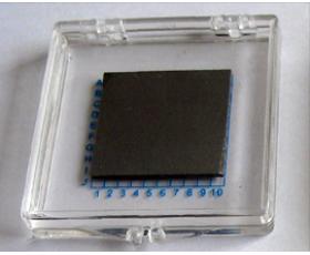
갈륨 비소 (갈륨 비소) 웨이퍼
선도적인 GaAs 기판 공급업체인 PAM-XIAMEN은 프라임 등급 및 더미 등급의 반도체 n형, 반도체 C 도핑 및 p형을 포함한 Epi-ready GaAs(갈륨 비소) 웨이퍼 기판을 제조합니다. GaAs 기판 저항률은 도펀트에 따라 달라지며, Si 도핑 또는 Zn 도핑은 (0.001~0.009) ohm.cm이고, C 도핑은 >=1E7 ohm.cm입니다. GaAs 웨이퍼 결정 방향은 (100)과 (111)이어야 합니다. (100) 방향의 경우 2°/6°/15° 어긋날 수 있습니다. GaAs 웨이퍼의 EPD는 일반적으로 LED의 경우 <5000/cm2이고 LD 또는 마이크로 전자공학의 경우 <500/cm2입니다.
- 기술
제품 설명
(갈륨 비소) GaAs 웨이퍼
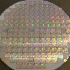
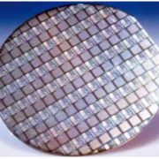
PAM-XIAMEN은 화합물 반도체 기판-갈륨 비소 결정 및 웨이퍼를 개발하고 제조합니다. 우리는 고급 결정 성장 기술, VGF(Vertical Gradient Freeze) 및 GaAs 웨이퍼 제조 공정을 사용하고 결정 성장, 절단, 연마, 연마 공정에 이르는 생산 라인을 구축하고 GaAs 웨이퍼 세척 및 패키징을 위한 100 클래스 클린룸을 구축했습니다. 당사의 GaAs 웨이퍼에는 LED, LD 및 Microelectronics 응용 분야를 위한 2~6인치 잉곳/웨이퍼가 포함됩니다. 우리는 현재 GaAs 웨이퍼 기판의 품질을 개선하고 대형 기판을 개발하기 위해 항상 최선을 다하고 있습니다. 제공되는 GaAs 웨이퍼 크기는 2”, 3”, 4” 및 6”이며 두께는 220-700um이어야 합니다. 또한 우리의 GaAs 웨이퍼 가격은 경쟁력이 있습니다.
1. GaAs 웨이퍼 사양
1.1(GaAs)갈륨 비소LED 애플리케이션 용 웨이퍼
| 명세서 | 비고 | |
| 전도 유형 | SC / n 형 | 아연 마약 사용 가능한에게 사우스 캐롤라이나 / p 형 |
| 성장 방법 | VGF | |
| 도펀트 | 규소 | 가능한 아연 |
| 웨이퍼을 직경 | 2, 3, 4 인치 | 잉곳 또는 컷 availalbe |
| 크리스탈 방향 | (100) 2 °/ 6 ° / 15 (110)를 오프 ° | 사용할 수있는 다른 탈각 |
| 의 | EJ 또는 미국 | |
| 캐리어 농도 | (2.5 ~ 0.4) E18 / cm3 | |
| RT에서 저항 | (1.5 ~ 9) E-3 Ohm.cm | |
| 유동성 | 1500 ~ 3,000cm2 / V.sec | |
| 에치 피트 밀도 | <5000 / cm2 | |
| 레이저 마킹 | 요청에 따라 | |
| 표면 처리 | P / E 또는 P / P | |
| 두께 | 220 ~ 450um | |
| 에피 택시 준비 | 예 | |
| 패키지 | 단일 웨이퍼 용기 또는 카세트 | |
1.2(GaAs)갈륨 비소LD 애플리케이션 용 웨이퍼
| 명세서 | 비고 | |
| 전도 유형 | SC / n 형 | |
| 성장 방법 | VGF | |
| 도펀트 | 규소 | |
| 웨이퍼을 직경 | 2, 3, 4 인치 | 잉곳 또는 사용 가능한 같은 컷 |
| 크리스탈 방향 | (100) 2 °/ 6 ° / 15 (110)를 오프 ° | 사용할 수있는 다른 탈각 |
| 의 | EJ 또는 미국 | |
| 캐리어 농도 | (2.5 ~ 0.4) E18 / cm3 | |
| RT에서 저항 | (1.5 ~ 9) E-3 Ohm.cm | |
| 유동성 | ~ 3000 1,500cm2 / V.sec | |
| 에치 피트 밀도 | <500 / cm2 | |
| 레이저 마킹 | 요청에 따라 | |
| 표면 처리 | P / E 또는 P / P | |
| 두께 | 220 ~ 350um | |
| 에피 택시 준비 | 예 | |
| 패키지 | 단일 웨이퍼 용기 또는 카세트 | |
1.3(GaAs)갈륨 비소웨이퍼는 마이크로 일렉트로닉스 애플리케이션을위한 세미 절연
| 명세서 | 비고 | |
| 전도 유형 | 절연 | |
| 성장 방법 | VGF | |
| 도펀트 | C 도핑 | |
| 웨이퍼을 직경 | 2, 3, 4 인치 | 잉곳 사용 가능 |
| 크리스탈 방향 | (100)+/- 0.5° | |
| 의 | EJ, 미국이나 노치 | |
| 캐리어 농도 | N / A | |
| RT에서 저항 | > 1E7 Ohm.cm | |
| 유동성 | > 5,000cm2 / V.sec | |
| 에치 피트 밀도 | <8000 / cm2 | |
| 레이저 마킹 | 요청에 따라 | |
| 표면 처리 | P / P | |
| 두께 | 350 ~ 675um | |
| 에피 택시 준비 | 예 | |
| 패키지 | 단일 웨이퍼 용기 또는 카세트 | |
1.4 6″ (150mm)(GaAs)갈륨 비소웨이퍼는 마이크로 일렉트로닉스 애플리케이션을위한 세미 절연
| 명세서 | 비고 | |
| 전도 유형 | 세미 절연 | - |
| 방법을 성장 | VGF | - |
| 도펀트 | C 도핑 | - |
| 유형 | N | - |
| Diamater (mm) | 150 ± 0.25 | - |
| 정위 | (100)0°±3.0° | - |
| 노치 방향 | 〔010〕 ± 2 ° | - |
| NOTCH Deepth (mm) | (1-1.25)mm 89°-95° | - |
| 캐리어 농도 | 영업팀에 문의하십시오. | - |
| 저항 (ohm.cm) | >1.0×10⁷ | - |
| 이동성 (cm2 / 대) | 영업팀에 문의하십시오. | - |
| 탈구 | 영업팀에 문의하십시오. | - |
| 두께 (μm의) | 675 ± 25 | - |
| 활과 워프 (mm)에 대한 에지 제외 | 영업팀에 문의하십시오. | - |
| 보우 (μm의) | 영업팀에 문의하십시오. | - |
| 워프 (μm의) | ≤20.0 | - |
| TTV (μm의) | ≤10.0 | - |
| TIR (μm의) | ≤10.0 | - |
| LFPD (μm의) | 영업팀에 문의하십시오. | - |
| 세련 | P / P 에피 준비 | - |
1.5 2″(50.8mm) LT-GaAs(낮은 온도에서 재배 한 갈륨 비소) 웨이퍼 사양
| 명세서 | |
| 전도 유형 | 세미 절연 |
| 방법을 성장 | VGF |
| 도펀트 | 하위:C 도핑 / Epi:언도핑 |
| 유형 | N |
| Diamater (mm) | 150 ± 0.25 |
| 정위 | (100)0°±3.0° |
| 노치 방향 | 〔010〕 ± 2 ° |
| NOTCH Deepth (mm) | (1-1.25)mm 89°-95° |
| 캐리어 농도 | 영업팀에 문의하십시오. |
| 저항 (ohm.cm) | >1.0×10⁷ 또는 0.8-9 x10⁻³ |
| 이동성 (cm2 / 대) | 영업팀에 문의하십시오. |
| 탈구 | 영업팀에 문의하십시오. |
| 두께 (μm의) | 675 ± 25 |
| 활과 워프 (mm)에 대한 에지 제외 | 영업팀에 문의하십시오. |
| 보우 (μm의) | 영업팀에 문의하십시오. |
| 워프 (μm의) | ≤20.0 |
| TTV (μm의) | ≤10.0 |
| TIR (μm의) | ≤10.0 |
| LFPD (μm의) | 영업팀에 문의하십시오. |
| 세련 | P / P 에피 준비 |
2. GaAs 웨이퍼 시장 및 응용
갈륨 비소는 중요한 반도체 재료입니다. III-V족 화합물 반도체와 아연 블렌드 결정 격자 구조에 속하며 격자 상수는 5.65×10⁻¹⁰m, 녹는점은 1237°C, 밴드 갭은 1.4전자 볼트입니다. 갈륨 비소는 집적 회로 기판, 적외선 감지기, 감마 광자 감지기 등을 만드는 데 사용할 수 있는 반 절연 고저항 재료로 만들 수 있습니다. 전자 이동도가 실리콘보다 5~6배 크기 때문에 SI GaAs 기판은 마이크로파 장치 및 고속 디지털 회로의 제조에 중요하게 사용되었습니다. 갈륨 비소로 제조된 반도체 장치는 고주파, 고온, 저온 성능, 저잡음 및 강한 내방사성이라는 이점을 가지고 있어 GaAs 기판 시장을 확대합니다.
3. GaAs 웨이퍼의 테스트 인증서는 필요한 경우 아래 분석을 포함할 수 있습니다.
1/갈륨 비소의 앞면과 뒷면을 포함한 표면 거칠기(나노미터).
2/갈륨 비소의 도핑 농도(cm-3)
갈륨비소(cm-2)의 3/EPD
4/갈륨 아르센디의 이동성(V.sec)
5/갈륨 비소의 X-선 회절 분석(로킹 곡선): 회절 반사 곡선 반치폭
6/갈륨 비소의 저온 광발광(발광 스펙트럼 범위 0.7-1.0μm): 4K 또는 5K의 온도 및 광 여기 밀도에서 근적외선 범위의 발광 스펙트럼에서 여기자 광발광의 비율 1W/cm2
7/투과율 또는 흡수 계수: 즉석에서 우리는 1064nm에서 도핑되지 않은 단결정 GaAs의 흡수 계수를 측정할 수 있습니다: <0.6423 cm-1, 그리고 이것은 1064nm에서 정확히 6.5mm 두께의 블랭크에 대해 33.2%의 투과 최소값에 해당합니다.
주목:
중국 정부는 반도체 칩을 만드는 데 사용되는 갈륨 재료(예: GaAs, GaN, Ga2O3, GaP, InGaAs 및 GaSb) 및 게르마늄 재료의 수출에 대한 새로운 제한을 발표했습니다. 2023년 8월 1일부터 이러한 자료의 수출은 중국 상무부로부터 허가를 받은 경우에만 허용됩니다. 여러분의 이해와 협조를 바랍니다!
당신은 또한 같은 수 있습니다 ...
-
플로트 존 단결정 실리콘
PAM-XIAMEN은 Float Zone 방식으로 얻은 Float Zone 실리콘 웨이퍼를 제공할 수 있습니다. 단결정 실리콘 막대는 플로트 존 성장을 통해 얻은 다음 단결정 실리콘 막대를 플로트 존 실리콘 웨이퍼라고 하는 실리콘 웨이퍼로 가공합니다. 영역 용융된 실리콘 웨이퍼는 플로팅 영역 실리콘 프로세스 동안 석영 도가니와 접촉하지 않기 때문에 실리콘 물질은 부유 상태에 있습니다. 따라서 실리콘의 플로팅 존 용융 과정에서 오염이 적습니다. 탄소 함량과 산소 함량이 낮고 불순물이 적으며 저항률이 높습니다. 전력 장치 및 특정 고전압 전자 장치의 제조에 적합합니다.
-
SiC 웨이퍼 기판
이 회사는 결정 성장, 결정 처리, 웨이퍼 처리, 연마, 세척 및 테스트를 통합하는 완전한 SiC(탄화규소) 웨이퍼 기판 생산 라인을 보유하고 있습니다. 요즘 우리는 축상 또는 축외에서 반절연 및 전도성을 갖춘 상용 4H 및 6H SiC 웨이퍼를 공급합니다. 사용 가능한 크기: 5x5mm2,10x10mm2, 2",3",4", 6" 및 8", 다음과 같은 핵심 기술을 통해 돌파 결함 억제, 종결정 가공 및 급속 성장으로 실리콘 카바이드 에피택시, 소자 등과 관련된 기초 연구 및 개발을 촉진합니다.
-
InP의 웨이퍼
PAM-XIAMEN은 낮은 도핑, N 유형 또는 반절연을 포함한 프라임 또는 테스트 등급의 VGF InP(인화인듐) 웨이퍼를 제공합니다. InP 웨이퍼의 이동도는 유형에 따라 다릅니다. 저도핑 웨이퍼>=3000cm2/Vs, N 유형>1000 또는 2000cm2V.s(도핑 농도에 따라 다름), P 유형: 60+/-10 또는 80+/-10cm2 /Vs(다른 Zn 도핑 농도에 따라 다름) 및 반모욕적인 경우>2000cm2/Vs인 경우, 인화인듐의 EPD는 일반적으로 500/cm2 미만입니다.
-
프리 스탠딩 GaN 기판
PAM-XIAMEN는 UHB-LED 및 LD위한 (질화 갈륨), GaN 기판 웨이퍼를 자립의 제조 기술을 확립했다. 수 소화물 기상 성장 (HVPE) 기술에 의해 성장 우리 GaN 기판은 낮은 결함 밀도를 갖는다.
-
CdZnTe (CZT) 웨이퍼
카드뮴 아연 텔루 라이드 (CdZnTe 또는 CZT)을 효과적으로 일렉트론 방사선을 변환 할 수있는 새로운 반도체이며, 그것은 주로 적외선 박막 에피 택셜 기판, X 선 검출기 및 감마선 CdZnTe 검출기에 사용된다. -
갈륨 비소 에피 웨이퍼
PAM-XIAMEN은 MBE 또는 MOCVD에 의해 성장된 Ga, Al, In, As 및 P를 기반으로 다양한 유형의 에피 웨이퍼 III-V 실리콘 도핑 n형 반도체 재료를 제조하고 있습니다. 우리는 고객 사양을 충족하기 위해 맞춤형 GaAs 에피 웨이퍼 구조를 공급합니다. 자세한 내용은 당사에 문의하십시오.
-
창 (게르마늄) 싱글 수정 및 웨이퍼
PAM-XIAMEN은 2”, 3”, 4” 및 6” 게르마늄 웨이퍼를 제공하며, 이는 VGF/LEC에 의해 성장된 Ge 웨이퍼의 줄임말입니다. 약하게 도핑된 P 및 N 유형 게르마늄 웨이퍼도 홀 효과 실험에 사용할 수 있습니다. 실온에서 결정질 게르마늄은 부서지기 쉽고 가소성이 거의 없습니다. 게르마늄은 반도체 특성을 가지고 있습니다. 고순도 게르마늄에 3가 원소(인듐, 갈륨, 붕소 등)를 도핑하여 P형 게르마늄 반도체를 얻는다. 안티몬, 비소, 인 등의 5가 원소를 도핑하여 N형 게르마늄 반도체를 얻는다. 게르마늄은 높은 전자 이동도 및 높은 정공 이동도와 같은 우수한 반도체 특성을 가지고 있습니다. -
나노 제조 포토레지스트
PAM-하문은 포토 레지스트와 포토 레지스트 판을 제공