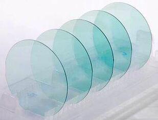
GaN epitaxy template on Sapphire substrate with N-type, P-type or semi-insulating is available for the preparation of semiconductor optoelectronic devices and electronic devices. GaN epitaxial layer on sapphire substrate refers to a composite structure composed of a gallium nitride single crystal thin film material and the supporting sapphire substrate, that after a series process operations such as epitaxial deposition, diffusion, and ion implantation. Especially pointed out that non-PSS (so-called SSP) templates are to co-load with PSS wafers for planar runs, which can help to more clearly see reflectance. The GaN on sapphire lattice mismatch from PAM-XIAMEN is relatively low. For more specifications of the GaN material epitaxy on Sapphire, please see the followings:
1. 사파이어 기판에 GaN 에피택시 템플릿의 웨이퍼 사양
1.1 사파이어의 도핑되지 않은 GaN 템플릿
사파이어의 GaN 템플릿, C 평면 5×5mm x 30미크론 두께, 1sp
사파이어의 GaN 템플릿, R-평면, 5 x 5mm x 5미크론,1sp
사파이어의 GaN 템플릿, C 평면, 10 x 10 mm x 5 미크론, 1sp
사파이어의 GaN 템플릿, M 평면, 10 x 10 mm x 5 미크론, 1sp
사파이어의 GaN 템플릿, C 평면, 10×10 x0.5 mm, 필름: 30 마이크론 두께
사파이어의 GaN 템플릿(C 평면), N형, 도핑되지 않음, 4″x 4-5 미크론,1sp
사파이어의 GaN 템플릿(C 평면), N형, 도핑되지 않은, 4″x 5 마이크론, 2sp
사파이어의 GaN 템플릿(C 평면), N형, 도핑되지 않은, 4″x 30 마이크론, 1sp(생산 등급)
사파이어의 GaN 템플릿(C 평면), N형, 도핑되지 않음, 2″x 4-5 미크론,1sp
사파이어의 GaN 템플릿(C 평면), N형, 도핑되지 않음, 2″x 5 마이크론, 2sp
사파이어의 GaN 템플릿(C 평면), N형, 도핑되지 않음, 2″x 30 마이크론, 1sp(생산 등급)
사파이어(C 평면)의 반 모욕적인 GaN 템플릿, N형, 도핑되지 않은, 4″x 5 미크론, 1sp
사파이어(C 평면)의 반모욕 GaN 템플릿, N형, 도핑되지 않음, 3″x 5 미크론, 1sp
사파이어의 GaN 템플릿(반절연) 4″x 20 마이크론–생산 등급
사파이어의 GaN 템플릿(반절연) 4″x 5 마이크론–연구 등급
사파이어의 GaN 템플릿(반절연) 2″x 20 마이크론–생산 등급
사파이어의 GaN 템플릿(반절연) 2″x 5 마이크론–연구 등급
1.2 사파이어에 도핑된 GaN 템플릿
사파이어에 GaN(0001) 템플릿(N+,Si 도핑), 4″x 5um,1sp
사파이어에 GaN(0001) 템플릿(N+,Si 도핑), 4″x 5um,2sp
사파이어에 GaN(0001) 템플릿(N형, Fe 도핑), 4″x 5um,1sp
사파이어에 GaN(0001) 템플릿(N+,Si 도핑), 2″x 5um,1sp
사파이어에 GaN(0001) 템플릿(N+,Si 도핑), 2″x 5um,2sp
사파이어에 GaN(0001) 템플릿(N형, Fe 도핑됨), 2″x 5um,1sp
사파이어 N+형의 Si 도핑 GaN(0001) 템플릿, 4″x 5 마이크론, 1sp
사파이어 N+에 FLAAT GaN(0001) 템플릿(N+, Si 도핑), 2″x 15um,1sp
사파이어 10x10x 2 마이크론, 1sp의 Mg 도핑된 P형 GaN(0001) 템플릿, 도핑 농도: 5E17/cc
사파이어 4″ x 2 마이크론, 1sp의 Mg 도핑된 P형 GaN(0001) 템플릿, 도핑 농도: 5E17/cc
Mg 도핑된 P형 GaN(0001) 사파이어 4″ x 2 미크론, 2sp의 에피택셜 템플릿
사파이어 2″ x 2 마이크론, 1sp의 Mg 도핑된 P형 GaN(0001) 템플릿, 도핑 농도: 5E17/cc
Mg 도핑된 P형 GaN(0001) 사파이어 2″ x 2 마이크론의 에피택시 템플릿, 2sp
2. 사파이어 상의 에피택시 GaN 필름에 대한 산업 기준
This standard applies to the preparation of templates of GaN epi-layer on sapphire for semiconductor optoelectronic devices and electronic devices.
2.1 사파이어에서 GaN 에피택셜 성장의 휨
테이블의 Y, Z, H에 대한 참고 사항:
"Y" – 두께가 20um(포함)을 초과하지 않는 사파이어의 질화갈륨 에피택시 템플릿.
"Z" - 두께가 20um를 초과하지만 50um(포함)을 초과하지 않는 사파이어 기반 GaN 에피택셜 웨이퍼.
"H" – 두께가 50um 이상인 사파이어 웨이퍼의 GaN.
사파이어 위의 GaN 에피웨이퍼의 휨은 표 1의 요구 사항을 충족해야 합니다.
표 1 사파이어 상의 GaN 에피택셜 필름의 휨
| 두께 코드 | 경사 |
| Y | ≤200 음 |
| Z | ≤300 음 |
| H | ≤500 음 |
2.2 사파이어 기반 GaN 에피택셜 성장을 위한 두께
사파이어 에피택시의 N-극성 GaN 두께는 표 2의 요구 사항을 준수해야 합니다.
표 2 GaN 층 두께 및 총 두께 변화
| 두께 코드 | 두께 편차 | TTV |
| y | ±2음 | ≤2 음 |
| Z | ±5음 | ≤5 음 |
| H | ±10음 | ≤10 음 |
2.3 사파이어 기판에서 질화갈륨 에피택시의 표면 품질
The surface of sapphire based gallium nitride epitaxial growth should be a mirror-like, no yellowing, no blackening, and no chromatic aberration. And surface defects of SSP template should meet the requirements of Table 3.
표 3 표면 결함의 최대 허용 값
| 최대 허용 값 | ||
| 2인치 | 4인치 | |
| 얼룩 | 없음 | 없음 |
| 스크래치(수량: 스트립, 스크래치 길이: mm) | ≤2: ≤5mm | ≤5: ≤5mm |
| 균열, 오리 발톱, 잔물결, 오렌지 껍질, 안개, 부서진 가장자리 | 없음 | 없음 |
| 작은 언덕과 구덩이 (Dia≥0.5mm, 단위: pcs/cm2) | 없음 | 없음 |
| 작은 언덕 및 구덩이 (0.2mm≤직경<0.5mm, 단위: 개) | 1 | 2 |
| 참고: 표면 결함 영역은 가장자리에서 제거된 2mm 링 영역의 전체 표면을 나타냅니다. | ||
The surface roughness of epitaxy of gallium nitride on sapphire wafer should be less than 0.6nm.
고객이 특정 품목에 대해 특별한 요구가 있는 경우 공급자와 구매자가 결정해야 합니다.
2.4 사파이어 전기 매개변수의 GaN 에피 웨이퍼
사파이어 템플릿의 단결정 GaN 에피택시의 전기적 매개변수는 표 4의 요구 사항을 충족해야 합니다.
표 4 전기적 매개변수
| 전도도 유형 | 캐리어 농도 cm-3 | 기동성 cm3/V1- NS1 | 저항 ohm- cm |
| N 형 | >1×10¹⁸ | ≥150 | <0.05 |
| P 형 | >1×10¹⁷ | ≥5 | <1 |
| 세미 절연 | – | – | ≥106 |
2.5 사파이어 피크 위치 및 반폭에서의 GaN 에피택시
GaN 에피택시 템플릿의 피크 위치 및 반치폭의 허용 값은 표 5의 요구 사항을 충족해야 합니다.
표 5 피크 위치 및 절반 너비
| 수정면 | 피크 위치(브래그 각도) | FWHM (아크 초) |
| ( 10-12) | 24.04°+/- 0.6°(제품 요구의 편향각에 의해 결정됨) | ≤250 |
| (0002) | 17.28°+/- 0.6°(제품 요구의 편향각에 의해 결정됨) | ≤250 |
3. FAQ of GaN on Sapphire Template
Q1: Why you have carrier concentration less than dopant density of GaN on sapphire epitaxy?
A: For GaN epitaxy on sapphire wafer, Mg and H will be combined, about 1/1000 will be activated, and the activation energy is higher, so the doping concentration is greater than the carrier concentration.
Q2: Since I will be doing high-temperature solar cells with your p-GaN, will the carrier concentration be stable at 400 degree-C?
A: The 400 degree is high a bit, and I think it can be affordable at a short time at 400 degrees,but the efficiency will decline for a long time.Of course, it also depends on your device structure. If it’s just a very simple PN structure, no quantum well may be better. In addition, the Mg activation of the P type can also be achieved by annealing at high temperature.
Q3: Can you please inform me what is the minimum thickness of p-GaN you can provide? Can I get at least 5-7micro-meter of p-GaN?
A: The constant thickness is as below we mentioned: in the market, when people say 5um p type GaN, actually it includes all the layers p-gan, u-gan, and GaN buffer, here clearly say the market 5um p gan is just our wafers.
2/GaN epitaxy on sapphire, p type
2″ dia, p-type, Mg doped ,
Total thickness :>4.5um+/-0.5um
Orientation: C-axis(0001)+/-1O
Substrate Structure:
p-GaN(>=2.0um)
u-GaN(2.0-2.5um)
GaN Buffer layer
Sapphire(430um,S.P.)
Surface Finish :Single Side Polished,epi-ready
Usable Area ≥ 90 %
Q4: I want to know if you cut the wafer from undoped GaN template on sapphire wafer of make it in 10x10mm size? and how you clean it ? because I used chemical solution and it increase the roughness, so how can I clean GaN epitaxy template without any damage for surface or when I receive it from you it clean and I can used it? this information very important for my research.
A: The regular process for undoped GaN on Sapphire template after cutting them by laser:
- put the substrate in the cleaning container.
- pour acetone, the capacity of acetone should be soaked at 2mm and ultrasonic cleaning for 10 minutes.
- the acetone is poured into the waste liquid bucket and poured into the anhydrous ethanol. The capacity of the anhydrous ethanol should be immersed in the height of 2mm, and the ultrasonic cleaning is 10 minutes.
- will be used back into the waste liquid bucket and deionized water for 10 times.
- preparation of No. 1 liquid (H2O2:NH3.H2O:H2O=2:1:7), deionized water for boiling water, cleaning for 5 minutes;
- deionized water rinse 10 times;
- blow dry (100 grade clean table);
Q5: Please tell me the roughness of the undoped GaN epitaxy template on sapphire, and how can I order 1x1cm samples from your company. And its growth by HVPE?
A: The roughness of undoped GaN epitaxy on Al2O3: Ra<2nm, it is natural growth surface, by MOCVD.

자세한 내용은 다음 주소로 이메일을 보내주십시오. victorchan@powerwaywafer.com 과 powerwaymaterial@gmail.com.