추상
고급 특성화는 태양 전지의 비용 효율성($/Wp)을 추가로 개선하는 데 중요한 역할을 합니다. 이 문서는 현재 분석에 사용되는 고급 특성화 기술의 개요를 제공합니다.실리콘 웨이퍼 태양 전지, 실험실이나 공장에서. 다루는 기술은 다음과 같습니다.
발광 이미징, 수명 분광법, 광학 및 전기 측정. 우리는 전적으로 측정된 매개변수를 기반으로 하는 상세한 손실 분석을 제시하며, 이는 실리콘 웨이퍼 태양 전지의 주요 손실 프로세스를 정량화합니다. 이 손실 분석은 완전히 고정밀 측정을 기반으로 하며 상세한 정량화(in
W/cm2) 전면 금속 음영, 활성 영역의 전면 반사, 전면 탈출, 직렬 및 션트 저항, 불완전 활성 영역 내부 양자 효율 및 순방향 바이어스로 인한 태양 전지의 전력 손실 1-sun 최대 전력점에서의 전류. 우리는 또한 철저한 특성화를 보여줍니다.
개별 처리 단계와 최종 태양 전지의 상세한 손실 분석을 사용하여 산업용 실리콘 웨이퍼 태양 전지의 평균 효율과 수율을 향상시킬 수 있습니다.
1. 소개
현재 실리콘 웨이퍼 태양전지가 시장을 장악하고 있으며 시장 점유율은 더욱 높아지고 있다. 이러한 태양 전지의 압도적인 대다수는 다음 단계로 구성된 제조 순서로 생산됩니다.
나. 톱 손상 제거를 포함한 표면 질감
ii. 인 확산(튜브 또는 인라인 확산)
iii. 인 규산염 유리 제거
iv. 질화규소 증착
v. 전면 및 후면 금속 접점의 스크린 인쇄
vi. 에지 격리
모든 산업용 태양 전지에 대해 태양 에너지 변환 효율이 측정됩니다. 그러나 실리콘 웨이퍼 태양 전지의 완성 전후에 실리콘 샘플에서 상당한 양의 정보를 얻을 수 있습니다. 이 문서에서는 부분적으로 처리된 실리콘 웨이퍼에서 추출할 수 있는 몇 가지 일반적인 프로세스 관련 문제를 제시합니다. 또한, 7가지 가장 중요한 손실 메커니즘을 정량화하는 완성된 실리콘 웨이퍼 태양 전지에 대한 상향식 손실 분석이 제공됩니다. 이 방법
실리콘 웨이퍼 태양 전지의 최적화 가이드 역할을 할 수 있습니다.
2. 부분적으로 처리된 실리콘 웨이퍼의 특성화
2.1. 광발광 이미징에 의한 원시 웨이퍼 분석
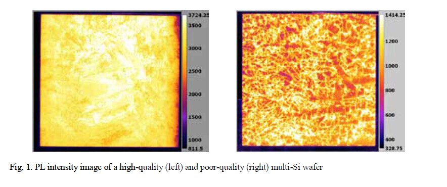
Photoluminescence (PL) imaging has emerged in the last decade as a very versatile characterisation technique in the field of silicon wafer photovoltaics [1]. Of particular interest is that PL enables us to study partly processed silicon wafers in every step of the solar cell fabrication sequence. As an example, Fig. 1 shows PL intensity images taken on a high-quality and a low-quality multi-Si wafer (PL images taken with the LIS-R1 system from BT Imaging, Australia). The wafers were measured in their as-received state, i.e. no processing step was applied at SERIS. The high-quality wafer has a uniform appearance, apart from a lower intensity edge at the right which can be attributed to the block-casting process. The low-quality wafer has a clearly different appearance with a significant portion of the wafer appearing “dark”. It has been shown by Giesecke et al. that dark areas in raw wafers relate to areas with bulk minority carrier lifetimes of < 10 s [2]. Interestingly, the areas close to the grain boundaries are brighter in the PL image of the low-quality multi-Si wafer. This can be explained by the internal gettering of impurities by the grain boundaries, resulting in higher effective lifetimes in the proximity of grain boundaries in multi-Si with a high impurity content. This multi-Si wafer was clearly cut from either the top or bottom of the ingot. This result clearly shows that PL has the potential to assess the quality of as-received wafers before any processing. This information can be used for incoming quality control or to “bin” the incoming wafers into quality groups and to tailor especially the thermal processing in order to get the optimal cell efficiency for each quality group, instead of processing all wafers in the same way.
2.2. Saw damage removal and texturing
The as-received silicon wafers contain a defective layer at each surface (front and rear), as a result of the sawing process. The minority carrier lifetime in this saw-damaged layer is relatively low due to chemical impurities and crystal imperfections resulting from the sawing process. This defective layer is removed by chemical processing, typically in the same step that is used for texturing the surfaces of the silicon wafer. It is of key importance that the defective layer is completely removed in this chemical step.
그러나 결함층의 두께는 웨이퍼 공급업체마다 다르므로 결함층이 완전히 제거되도록 특성화 시퀀스가 필요합니다. 그림 2(a)에는 특정 실리콘 웨이퍼 유형에 대해 필요한 최소 SDE(톱 손상 에칭) 시간을 추출할 수 있는 프로세스 흐름이 나와 있습니다. 대칭적으로 부동태화된 수명 구조는 다양한 SDE 시간(80oC에서 KOH)을 받은 Si 웨이퍼에서 준비됩니다. 결과적으로 유효 수명은 예를 들어 준정상 상태 광전도 감쇠(WCT-120, Sinton Consulting, USA)[3])에 의해 결정됩니다. 그림 2(b)에서 우리는 이 특정 유형의 웨이퍼에 대해 최소 SDE 시간이 4분임을 알 수 있습니다.
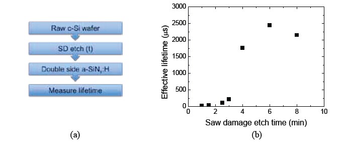
그림 2. (a) 실리콘 웨이퍼에 필요한 최소 톱 손상 에칭 시간을 결정하는 데 사용되는 실험 공정 흐름. (b) 대칭적으로 부동태화된 수명 샘플의 유효 소수 캐리어 수명은 톱 손상 에칭 시간을 증가시키기 위해 크게 증가합니다. 이 유형의 Si 웨이퍼의 경우 4의 최소 톱 손상 에칭 시간
분을 사용해야 합니다.
2.3. 인 확산
에미터 형성을 위한 표준 방법은 인라인 또는 튜브 확산에 의한 인 확산입니다. P 확산의 주요 매개변수는 시트 저항의 절대값과 측면 균일도입니다. 그림 3에는 모노-Si 웨이퍼에서 4점 프로브(Crestbox, Napson, Japan)를 사용하여 49개의 개별 측정을 수행하여 얻은 시트 저항 맵이 나와 있습니다. 이 특정 웨이퍼의 경우 균일성이 상대적으로 좋지 않아 전면 Ag 금속화에서 접촉 문제가 발생할 수 있습니다. 이 경우 모노-Si 웨이퍼는 웨이퍼 후면으로 도펀트 확산을 최소화하기 위해 연속적으로 로드되었습니다. 그러나 PL 강도 이미지는 웨이퍼 후면의 기생 P 확산에 기인할 수 있는 웨이퍼 주변의 고강도 에지를 보여줍니다. 따라서 이 기생 확산은 태양 전지 제조 순서의 나머지 부분에서 고려되어야 합니다. 이는 전지의 션트 또는 후면의 불량한 접촉 또는 패시베이션을 초래할 수 있기 때문입니다.
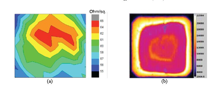
그림 3. (a) 목표 면저항이 60 Ohm/square인 156 mm 너비의 유사 정사각형 n+ 확산 p형 모노-Si 웨이퍼의 측정된 면저항 분포. 명백한 불균일성이 관찰되어 태양 전지 제조의 나중 단계에서 문제를 일으킬 수 있습니다. (b) 동일한 웨이퍼의 PL 강도 이미지는 더욱이
튜브 확산 공정으로 웨이퍼를 연속적으로 적재하는 것과 관련하여 웨이퍼 후면의 불균일.
2.4. 질화규소 증착
질화규소는 현재 막이 반사 손실을 줄이는 동시에 벌크 및 표면 패시베이션을 제공하기 때문에 실리콘 웨이퍼 태양 전지를 위한 최첨단 반사 방지 코팅(ARC)입니다. 최상의 표면 패시베이션 수준이 필름의 최상의 ARC 특성과 항상 일치하는 것은 아닙니다. 따라서 두 속성을 병렬로 처리해야 합니다. 그림 4에서 ARC와 표면 패시베이션 특성은 실리콘 질화물(SiNx) 필름의 굴절률의 함수로 표시됩니다. 광 흡수 및 반사 손실은 Ref. [4]. 텍스처 모노-실리콘 웨이퍼에서 질화규소 필름에 의해 유도된 반사 및 흡수 손실을 모두 고려하는 것이 중요하다는 것을 알 수 있습니다. 필름의 투과율은 이것이 태양 전지의 얻을 수 있는 전류를 제한하기 때문에 최적화되어야 합니다.

그림 4. (a) 알칼리 질감의 모노-Si 웨이퍼에서 SiNx 필름의 굴절률에 따른 가중 평균 반사, 흡수 및 투과율. SiNx 필름의 광학 두께는 150도로 일정하게 유지되었고 반사, 흡수 및 투과는 전송 매트릭스 방법과 함께 광선 추적을 사용하여 모델링되었습니다. 광학 손실은 AM1.5G 스펙트럼의 광자 플럭스에 의해 가중되었습니다. (b) SiNx 필름의 굴절률의 함수로서 양면에 70 Ohm/sq n+ 확산이 있는 SiNx 부동태화 텍스처 모노-Si 웨이퍼에서 광전도성 감쇠에 의해 측정된 에미터 포화 전류 밀도.
표면 패시베이션과 관련하여 다양한 실리콘 질화물 필름이 n형 에미터에서 우수한 수준의 표면 패시베이션을 제공하지만 필름이 표준 산업 소성에서 안정한 경우 주의를 기울여야 합니다. ARC와 패시베이션 특성을 모두 결합하여 최상의 실리콘 질화막을 선택할 수 있습니다(이 경우 굴절률이 2.0인 실리콘 질화막).
2.5. 스크린 인쇄 및 소성
일반적인 Si 웨이퍼 태양 전지의 전면 및 후면 금속 접점은 스크린 인쇄 및 소성로에서 접점의 후속 동시 소성으로 형성됩니다. 문제는 태양 전지의 전면과 후면에서 공간적으로 평균화된 낮은 전하 캐리어 재결합과 함께 낮은 직렬 저항을 얻는 것입니다. 또한, 태양 전지 전면의 금속화 분율을 최소화해야 합니다. 셀의 충전율과 직렬 저항을 모니터링하여 심각한 접촉 문제를 쉽게 파악할 수 있습니다(참조
섹션 3) 그러나 일부 프로세스 문제는 감지하기 위해 공간적으로 해결된 특성화가 필요합니다. 그림 5에는 태양 전지의 전면과 후면에 접촉 문제가 있는 Si 웨이퍼 태양 전지에 대한 두 개의 전계발광(EL) 강도 이미지가 나와 있습니다. 전면 금속 그리드 라인의 너비는 태양 전지 전면의 금속화 비율을 줄이기 위해 지속적으로 감소되고 있습니다. 그러나 이는 라인 컨덕턴스 또는 연결되지 않은 핑거로 인해 직렬 저항이 증가할 수 있습니다. 그림 5(a)에서
부러진 손가락은 EL 이미징으로 매우 쉽게 집어 올릴 수 있음을 알 수 있습니다. 후면 접촉의 접촉 및/또는 패시베이션 문제는 EL 이미지에서도 쉽게 확인할 수 있습니다(그림 5(b) 참조). 이 특정한 경우에 소성로의 금속 벨트의 거울 이미지가 이미지에서 볼 수 있으므로 최적화되지 않은 소성은 후면에서 국부적으로 불량한 접촉을 초래하여 태양 전지의 충전율을 감소시킵니다.
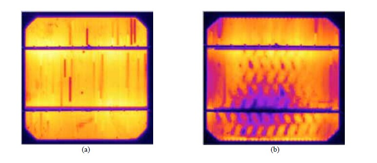
그림 5. (a) Ag 프론트 핑거가 파손된 모노-Si 웨이퍼 태양 전지의 EL 강도 이미지. (b) 후면 Al 접촉이 불량한 모노-Si 웨이퍼 태양 전지의 EL 강도 이미지.
3. 완성된 태양전지의 특성화
모든 태양 전지에 대해 one-sun IV 곡선이 측정되고 에너지 변환 효율이 결정됩니다. 그러나 태양 전지 연구자에게는 주어진 태양 전지의 효율을 제한하는 요인을 아는 것이 매우 중요합니다. 이러한 이유로 Si 웨이퍼 태양 전지에 대한 상향식 손실 분석을 수행하고 1-sun 최대 전력점(MPP)에서 태양 전지의 가장 중요한 7가지 손실 메커니즘을 정량화하는 새로운 방법이 SERIS에서 개발되었습니다. 셀의 직렬 저항 보정 MPP 전압(Vmpp)은 일정하게 유지됩니다[5]. 따라서 이 분석은 이론적인(그러나 실제로 달성할 수 없는) 태양 전지 효율 한계와 관련된 손실을 정량화하려는 것이 아닙니다. 대신 특정 태양 전지에서 지배적인 손실 메커니즘을 결정한 다음 개선된 버전의 태양 전지를 제작한 다음 손실 분석을 반복하는 등 반복적인 방식으로 사용하도록 의도되었습니다. 손실 분석 방법은 여기에서 18.1% 효율의 p-형 Cz 모노-Si 웨이퍼 태양 전지에서 시연됩니다.
SERIS에서 제작합니다. 전지는 전면에 균일한 n형 에미터가 있고 후면에 전체 영역 합금 후면 전계층이 있습니다. Ag 전면 및 Al 후면 접점 모두 스크린 인쇄되었습니다. SERIS 손실 분석에서 조사된 손실 메커니즘은 다음과 같습니다.
전면 금속 격자 음영
활성 영역의 전면 반사율;
전면 탈출
직렬 저항
션트 저항
불완전한 양자 효율
다이오드 재결합
먼저, 태양 전지의 전기적 특성이 결정됩니다. 이 작업에서는 슈퍼클래스 A 태양광 시뮬레이터(WXS-220S-L2, Wacom, Japan)가 있는 one-sun IV 테스터(SolSim-210, Aescusoft, Germany)를 사용했습니다. 광 JV 곡선(여기에는 표시되지 않음)에서 표준 태양 전지 매개변수가 유도됩니다. 개방 회로 전압 Voc, 단락 전류 밀도 Jsc, 충전 계수 FF, 효율 Eff, 최대 전력점 전압 Vmpp 및 최대 전력점 전류 밀도 Jmpp. 어두운 JV 곡선에서 션트 저항
is determined by a linear fit in the -50 mV to 50 mV range. By shifting the one-sun J-V curve by Jsc from the fourth to the first quadrant (shown in Fig. 6) and assuming that the solar cell obeys the superposition principle, the series resistance at the one-sun maximum power point (Rs.light) is determined from the voltage difference between the dark and the shifted one-sun J-V curve at Impp, as described by Aberle et al. [6]. Furthermore, the effective diode saturation current density J0.eff and the effective ideality factor neff are determined from the Rs-corrected light J-V curve. All these derived values are summarised in Table 1.
.jpg)

The quantum efficiency of the solar cell is determined in this work with the differential spectral response method, using a combination of modulated monochromatic light with steady-state white bias light [7]. The system used in this work (Fimo-210, Aescusoft, Germany) has a filter wheel based monochromator with 34 narrow-band filters and the linearity of the cell is checked prior to the measurement. The external and internal quantum efficiency for the metal-free area of the solar cell are shown in Fig. 7.
The metallised area of the cell’s front surface was measured using an automated 3D vision measurement system (MeasurVision, Sunny Instruments, Singapore). The reflectance Raa of the active cell area is subsequently calculated from the measured hemispherical reflectance (Lambda 950, PerkinElmer, USA), the measured metallisation fraction of the front surface, and the measured reflectance of the used front metal grid. The IQE of the active area (IQEaa) is then calculated using the measured metallisation fraction of the cell and the calculated Raa of the metal-free area. The IQEaa is used below for the quantification of the recombination losses in the short-circuited cell.
In the final part of the analysis the power losses (in mW/cm2) at the MPP of the solar cell are calculated for each of the seven studied loss mechanisms, assuming that the cell obeys the superposition principle. The optical losses and the losses due to a non-perfect IQEaa are calculated by weighting the measured data with the AM1.5G spectrum, whereby the calculated current loss at short circuit is converted into a power loss at MPP by multiplication with Vmpp. The resistive losses and the forward bias
current are calculated at MPP conditions, using the measured values of the solar cell from Table 1 and the one-diode equivalent circuit model. Our analysis thus assumes that the difference between Jsc and Jmpp is entirely due to the additional recombination triggered in the device by the forward bias voltage, which is true if the cell obeys the superposition principle and the shunt resistance is sufficiently high. The power loss results of this analysis are given in Table 2. As mentioned above, the analysis assumes that the series resistance corrected maximum power point voltage remains constant. It can be seen that for this particular cell the power loss due to the non-perfect IQEaa is dominant (37%), followed by the power loss due to front metal shading (24%). It can also be seen that the total current loss at MPP (12.6 mA/cm2) combined
with the measured Jmpp adds up to 47.2 mA/cm2, which is very close to the total possible current from the AM1.5G spectrum for wavelengths up to 1200 nm (47.0 mA/cm2). Hence, all major photon current loss processes have been accounted for.
4. Conclusions
In this paper we have shown that a significant amount of information can be extracted from partly processed silicon wafers, by applying a range of characterisation techniques. Furthermore we have presented a power loss analysis method for silicon wafer solar cells which quantifies the seven main power loss mechanisms at the cell’s maximum power point based on a bottom-up analysis. The method assumes that the Vmpp of the cell remains constant when the various loss mechanisms are eliminated; thus,
it should be used iteratively when improving solar cells, as the Vmpp will change as well. This analysis can easily be adapted to other photovoltaic technologies such as Si thin film, CIGS, and CdTe based solar cells, and to photovoltaic modules. As described in this paper, advanced characterisation plays a key role in improving the efficiency and yield of photovoltaic technologies.
References
[1] Trupke T, Bardos RA, Schubert MC, Warta W. Photoluminescence imaging of silicon wafers. Appl. Phys. Lett. 2006; 89:044107.
[2] Giesecke JA, The M, Kasemann M, Warta W. Spatially resolved characterization of silicon as-cut wafers with photoluminescence imaging. Prog. Photovolt. 2009; 17: 217.
[3] Sinton RA, Cuevas A. Contactless determination of current-voltage characteristics and minority-carrier lifetimes in semiconductors from quasi-steady-state photoconductance data. Appl. Phys. Lett. 1996; 69:2510.
[4] Duttagupta S, Ma F, Hoex B, Mueller T, Aberle AG. Optimised antireflection coatings using silicon nitride on textured silicon surfaces based on measurements and multidimensional modelling. Proc. International Conf. on Materials for
Advanced Technologies 2011, Symposium O, Singapore; Energy Procedia, 2011.
[5] Aberle AG, Zhang W, Hoex B. Advanced loss analysis method for silicon wafer solar cells. Proc. SiliconPV 2011 Conf. (1st International Conf. on Crystalline Silicon Photovoltaics), Freiburg, Germany; Energy Procedia, 2011, volume 8, p. 244-9.
[6] Aberle AG, Wenham SR, Green MA. A new method for accurate measurements of the lumped series resistance of solar cells. Proc. 23rd IEEE Photovoltaic Specialists Conf., Louisville, USA; 1993, p. 133-8.
[7] Metzdorf J. Calibration of solar cells. 1: The differential spectral responsivity method. Appl. Optics 1987; 26: 1701
Source:Sciencedirect
For more information, please visit our website:www.powerwaywafer.com, send us email at sales@powerwaywafer.com or powerwaymaterial@gmail.com