We are an expert of semiconductor wafers in semiconductor industry, and we offer technology support and wafers selling for thousands of univerisities and industrial customers by our decades experience, including Cornell University, Stanford Univeristy,Peking University, Shandong Univerity, university of south carolina,Caltech Faraon lab (USA),University of California, Irvine (USA),Singapore MIT Alliance for Research and Technology Centre (SMART),West Virginia University,Purdue Univerity, University of California, Los Angeles,King Abdullah University of Science & Technology,Massachusetts Institute of Technology,University of Houston,University of Wisconsin,University of Science and Technology of China etc.
And now we show one article example as follows, who bought our wafers or service:
Article title:Incipient plasticity in 4H-SiC during quasistatic nanoindentation
Published by:
Saurav Goel ;Jiwang Yan ;Xichun Luo ;Anupam Agrawald
a School of Mechanical and Aerospace Engineering, Queen’s University, Belfast BT95AH, UK
b Department of Mechanical Engineering, Keio University, Yokohama 223-8522, Japan
c Department of Design, Manufacture and Engineering Management, University of Strathclyde, Glasgow G11XQ, UK
d Department of Business Administration, University of Illinois at Urbana Champaign, 61820, USA
Picture of SiC wafer:
Abstract
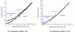
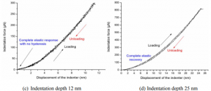
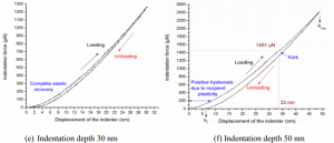
Silicon carbide (SiC) is an important orthopedic material due to its inert nature and superior mechanical and tribological properties. Some of the potential applications of silicon carbide include coating for stents to enhance hemocompatibility, coating for prosthetic-bearing surfaces and uncemented joint prosthetics. This study is the first to explore nanomechanical response of single crystal 4H-SiC through quasistatic nanoindentation. Displacement controlled quasistatic nanoindentation experiments were performed on a single crystal 4H-SiC specimen using a blunt Berkovich indenter (300 nm tip radius) at extremely fine indentation depths of 5 nm, 10 nm, 12 nm, 25 nm, 30 nm and 50 nm. Load–displacement curve obtained from the indentation experiments showed yielding or incipient plasticity in 4H-SiC typically at a shear stress of about 21 GPa (~an indentation depth of 33.8 nm) through a pop-in event. An interesting observation was that the residual depth of indent showed three distinct patterns: (i) positive depth hysteresis above 33 nm, (ii) no depth hysteresis at 12 nm, and (iii) negative depth hysteresis below 12 nm. This contrasting depth hysteresis phenomenon is hypothesized to originate due to the existence of compressive residual stresses (upto 143 MPa) induced in the specimen by the polishing process prior to the nanoindentation.
Subjuect(s):SiC ;Nanoindentation ;Plasticity ;Elastic response
Article abstract for Using Wafer from Xiamen Powerway Advanced Material Co. Ltd. (PAM-XIAMEN) or Powerway Wafer Co.,Limited
“… similar instruments. The specimen used was a single crystal 4H-SiC wafer having crystal orientation (001), diameter 50 mm and thickness 5 mm which was supplied by PAM-Xiamen Power-way Advanced Material Co. Ltd., China …”
Source:https://www.sciencedirect.com/science/article/pii/S1751616113004165
About Xiamen Powerway Advanced Material Co., Ltd
PAM-XIAMEN offers semiconductor silicon carbide wafers,6H SiC and 4H SiC wafer in different quality grades for researcher and industry manufacturers. We has developed SiC crystal growth technology and SiC wafer processing technology. We provide custom thin film (silicon carbide)SiC epitaxy on 6H or 4H substrates for the development of silicon carbide devices. SiC epi wafer is mainly used for Schottky diodes, metal-oxide semiconductor field-effect transistors, junction field effect.
PAM-XIAMEN also offer GaAs/InP and GaN material from wafer substrate to epitaxial growth.
Powerway Wafer Co.,Limited is a sub company of Xiamen Powerway Advanced Material Co., Ltd specialize in dealing with overseas orders.
Are You Looking for an Semiconductor wafer?
PAM-XIAMEN is proud to offer semiconductor wafer inlcuidng SiC/GaN/GaAs/InP wafer with wafer or epitaxial wafer for all different kinds of projects. If you are looking for semiconductor wafer, send us enquiry today to learn more about how we can work with you to get you the substrate wafers you need for your next project. Our group team is looking forward to providing both quality products and excellent service for you! For more information, please visit our website:www.powerwaywafer.com, send us email at tech@powerwaywafer.com or powerwaymaterial@gmail.com.