
Preparation and Performance Study of Ohmic Contact on SiC Wafer by Laser Annealing +
PAM-XIAMEN is able to provide various types of 4H-SiC epitaxial wafers. For details, please contact at [email protected]
With the development of power devices towards high integration and high power density, the substrate thickness of the devices continues to decrease to reduce series resistance, which poses higher requirements for the preparation process of backside ohmic contacts. The traditional rapid thermal annealing (RTA) process is carried out at high temperatures, which can easily lead to performance degradation of the device’s front side structure (such as Schottky contacts), and has a large thermal budget. In recent years, laser annealing technology has been widely studied and applied in the preparation of SiC ohmic contacts due to its advantages of local heating, small heat affected zone, and flexible process.
1. Mechanism and Parameter Optimization of SiC Laser Annealing Process
During the laser annealing process, parameters such as laser wavelength, energy density, number of pulses, and base temperature have a decisive impact on the formation of ohmic contacts. Research has shown that ultraviolet lasers with wavelengths below 355nm are more easily absorbed by metal electrodes, which is beneficial for local heating and promotes the reaction between metal and SiC. For example, Berger et al. annealed Ti/4H-SiC using a 355nm flat top laser and obtained a contact resistivity of 1.4 × 10⁻⁴Ω· cm² at an energy density of 4.25 J/cm².
Multi pulse laser annealing (MPLA) further reduces the energy density required to form low resistance contacts. Opprecht et al. found that at a base temperature of 400°C, a single pulse laser can achieve ohmic contact with a contact resistivity as low as 10⁻⁵Ω· cm². In addition, as the number of pulses increases, the silicide reaction advances and carbon redistribution becomes more uniform, which is beneficial for reducing contact resistance.
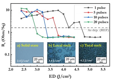
Fig. 1 Relationship between Rs and energy density under different pulse numbers
2. Reaction Between Electrodes and Silicides
The most widely studied ohmic contact metals at present are nickel (Ni) and titanium (Ti). Ni reacts with Si in SiC at high temperatures to form nickel silicon compounds (such as Ni₂Si, NiSi, NiSi₂), which are the basis for forming low resistance ohmic contacts. However, carbon clusters will precipitate during the Ni reaction process, affecting the metal adhesion and interface stability.
In contrast, Ti can react with Si and C in SiC to form Ti5Si3 and TiC, effectively suppressing carbon precipitation and improving interface quality. De Silva et al. prepared Ti-Si-C epitaxial contacts on C-plane 4H-SiC by pulsed laser annealing, and obtained a contact resistivity of 7.9 × 10⁻⁵Ω·cm².
XRD and TEM analysis indicate that the silicide phase formed during laser annealing is closely related to the contact resistance. Badala et al. found that as the degree of substrate damage increases, the silicide reaction transitions from a nickel rich phase (such as Ni₃₅Si) to a nickel poor phase (such as Ni₂₅Si), and the contact resistance decreases accordingly.
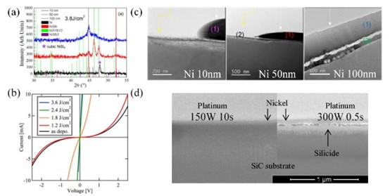
Fig. 2 Comparison of XRD and TEM interface structures between Ni and Ti electrodes
3. Effects of Substrate Thinning and Crystal Damage
Substrate thinning is a key step in reducing the series resistance of devices, but mechanical grinding can introduce surface roughness and sub surface crystal damage, which in turn affects the formation of ohmic contacts. Badala et al. systematically studied the effects of three thinning processes, namely coarse grinding, fine grinding, and ultrafine grinding, on the ohmic contact properties of Ni/4H-SiC.
Research has found that as surface roughness and defect density increase, the silicide reaction becomes more complete under the same laser conditions, and the contact resistance significantly decreases. TEM analysis shows that the thickness of the silicide layer in the rough ground sample is uneven, and there is still crystal damage at the interface. However, the reaction interface extends downwards at the defect, providing more Si sources available for the reaction.
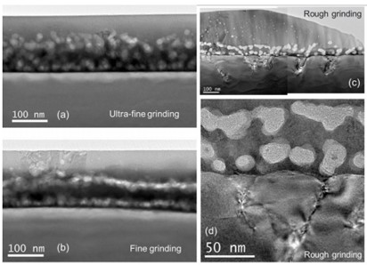
Fig. 3 TEM cross-section of silicide layer under different thinning processes
4. Accurate Characterization of Ohmic Contacts’ Electrical Properties
The performance of Ohmic contacts is usually evaluated by Specific Contact Resistance (SCR), and the Circular Transmission Line Method (c-TLM) is a commonly used measurement method. However, Berger et al. pointed out that directly fabricating TLM structures on highly doped SiC substrates can lead to current diffusion in the substrate, which cannot accurately reflect the true resistance of the contact interface.
Through TCAD simulation, they proposed inserting a low doping isolation layer (such as a 10μm thick, n⁻ layer with 5 × 10¹³cm⁻³ dopant) between the substrate and the contact layer, which can effectively limit the flow of current in the top n⁺ layer and accurately measure SCR values as low as 10⁻⁶ Ω· cm². This conclusion provides important basis for the precise characterization of laser annealed ohmic contacts.
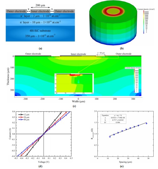
Fig. 4 Simulation diagram of current density distribution in 4H-SiC wafer with isolation layer structure
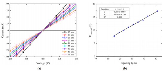
Fig. 5 I-V characteristics of Ti/4H-SiC contact and relationship between the resistance and spacing measured in the experiment
5. Verification of Laser Annealed Ohmic Contact Performance and Application Prospects
Laser annealed ohmic contacts have been validated in devices such as SiC Schottky barrier diodes (SBDs) and junction barrier Schottky diodes (JBS). Kim et al. compared laser annealed and RTA treated JBS devices and found that the forward turn-on voltage of laser annealed samples was lower, and the reverse breakdown voltage was higher.
Rusch et al. reported the preparation of 6A/650V SiC diodes using substrate thinning and laser annealing processes. The turn-on voltage decreased from 1.78V in RTA process to 1.62V, and the leakage current was less than 1μA at rated voltage. These results indicate that laser annealing technology has significant advantages in improving device performance.
Laser annealing, as a localized, low-temperature, and efficient annealing technique, has shown great potential in the preparation of ohmic contacts for SiC power devices. By optimizing laser parameters, electrode materials, and substrate processing techniques, high-quality ohmic contacts with contact resistivity below 10⁻⁵Ω· cm² can be achieved.

Whether you need SiC wafer for research or for industrial applications, please contact us email at [email protected] and [email protected].
References:
1. Li, G., Xu, M., Zou, D., Cui, Y., Zhong, Y., Cui, P., … & Han, J. (2023). Fabrication of Ohmic contact on N-Type SiC by laser annealed process: a review. Crystals, 13(7), 1106.
2. Opprecht, M., Kerdilès, S., Biscarrat, J., Godignon, P., Masante, C., Laviéville, R., … & Tabata, T. (2024). Ni/4H-SiC Ohmic Contact Formation Using Multipulse Nanosecond Laser Annealing. Solid State Phenomena, 359, 65-70.
3. Badalà, P., Bongiorno, C., Fiorenza, P., Bellocchi, G., Smecca, E., Vivona, M., … & Alberti, A. (2024). Electrical and structural properties of ohmic contacts of sic diodes fabricated on thin wafers. Solid State Phenomena, 359, 97-103.
4. Berger, C., Alquier, D., & Michaud, J. F. (2024). How to accurately determine the ohmic contact properties on n-type 4H-SiC. Electronics, 13(1), 217.