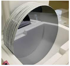
PAM-XIAMEN’ product line includes single-sided polishing (SSP) and double-sided polishing (DSP) wafer substrate or called mirror polished wafer for applications of semiconductors, MEMS, and other chips that require a strictly controlled flatness often require double-sided polishing chips. They are also necessary for a two-sided pattern and device manufacturing project. Normally end users will buy double side polished wafers due to better flatness. The roughness surface of polishing wafer should be required to Ra<0.5nm or 0.2nm.
반도체 장치는 계속 축소되고 있지만 칩이 앞면과 뒷면 모두에서 높은 표면 품질을 갖는 것이 점점 더 중요 해지고 있습니다. 현재 이러한 칩은 MEMS (Microelectro Mechanical System) 및 엄격한 평탄도 요구 사항이있는 애플리케이션에서 가장 일반적으로 사용됩니다. PAM-XIAMEN은 직경이 50mm에서 150mm에 이르는 다양한 양면 연마 웨이퍼를 제공합니다. 재고에 귀하의 사양이없는 경우 특정 사양에 맞게 웨이퍼를 맞춤화 할 수있는 여러 공급 업체와 장기적인 관계를 구축했습니다.
1. Polishing Wafer List of Silicon Carbide
| 4 ″ 4H 실리콘 카바이드 | |||||||
| 제품 번호. | 유형 | 정위 | 두께 | 학년 | 마이크로 파이프 밀도 | 표면 | 사용 가능 지역 |
| N 형 | |||||||
| S4H-100-N-SIC-350-A | 4 인치 4H-N | 0 ° / 39 ° ± 0.5 ° | 350 ± 25um | A | <10 / cm2 | P / P | > 90 %의 |
| S4H-100-N-SIC-350-B | 4 인치 4H-N | 0 ° / 39 ° ± 0.5 ° | 350 ± 25um | B | <30 / cm2 | P / P | > 85 %의 |
| S4H-100-N-SIC-350-D | 4 인치 4H-N | 0 ° / 39 ° ± 0.5 ° | 350 ± 25um | D | <100 / cm2 | P / P | > 75 %의 |
| S4H-100-N-SIC-370-L | 4 인치 4H-N | 0 ° / 39 ° ± 0.5 ° | 370 ± 25um | D | * | L / L | > 75 %의 |
| S4H-100-N-SIC-440-AC | 4 인치 4H-N | 0 ° / 39 ° ± 0.5 ° | 440 ± 25um | D | * | 로 컷 | > 75 %의 |
| S4H-100-N-SIC-C0510-AC-D | 4 인치 4H-N | 0 ° / 39 ° ± 0.5 ° | 5 ~ 10mm | D | <100 / cm2 | 로 컷 | * |
| S4H-100-N-SIC-C1015-AC-C | 4 인치 4H-N | 0 ° / 39 ° ± 0.5 ° | 5 ~ 10mm | C | <50 / cm2 | 로 컷 | * |
| 3 ″ 4H 실리콘 카바이드 | |||||||
| 제품 번호. | 유형 | 정위 | 두께 | 학년 | 마이크로 파이프 밀도 | 표면 | 사용 가능 지역 |
| N 형 | |||||||
| S4H-76-N-SIC-350-A | 3 인치 4H-N | 0 ° / 39 ° ± 0.5 ° | 350 ± 25um | A | <10 / cm2 | P / P | > 90 %의 |
| S4H-76-N-SIC-350-B | 3 인치 4H-N | 0 ° / 39 ° ± 0.5 ° | 350 ± 25um | B | <30 / cm2 | P / P | > 85 %의 |
| S4H-76-N-SIC-350-D | 3 인치 4H-N | 0 ° / 39 ° ± 0.5 ° | 350 ± 25um | D | <100 / cm2 | P / P | > 75 %의 |
| S4H-76-N-SIC-370-L | 3 인치 4H-N | 0 ° / 39 ° ± 0.5 ° | 370 ± 25um | D | * | L / L | > 75 %의 |
| S4H-76-N-SIC-410-AC | 3 인치 4H-N | 0 ° / 39 ° ± 0.5 ° | 410 ± 25um | D | * | 로 컷 | > 75 %의 |
| S4H-76-N-SIC-C0510-AC-D | 3 인치 4H-N | 0 ° / 39 ° ± 0.5 ° | 5 ~ 10mm | D | <100 / cm2 | 로 컷 | * |
| S4H-76-N-SIC-C1015-AC-D | 3 인치 4H-N | 0 ° / 39 ° ± 0.5 ° | 10 ~ 15mm | D | <100 / cm2 | 로 컷 | * |
| S4H-76-N-SIC-C0510-AC-C | 3 인치 4H-N | 0 ° / 39 ° ± 0.5 ° | 5 ~ 10mm | C | <50 / cm2 | 로 컷 | * |
| S4H-76-N-SIC-C1015-AC-C | 3 인치 4H-N | 0 ° / 39 ° ± 0.5 ° | 10 ~ 15mm | C | <50 / cm2 | 로 컷 | * |
| 반 절연 |
| S4H - 76 SI-SIC-350-A | 3 인치 4H-SI | 0 ° / 39 ° ± 0.5 ° | 350 ± 25um | A | <10 / cm2 | P / P | > 90 %의 |
| S4H - 76 SI-SIC-350-B | 3 인치 4H-SI | 0 ° / 39 ° ± 0.5 ° | 350 ± 25um | B | <30 / cm2 | P / P | > 85 %의 |
| S4H - 76 SI-SIC-350-D | 3 인치 4H-SI | 0 ° / 39 ° ± 0.5 ° | 350 ± 25um | D | <100 / cm2 | P / P | > 75 %의 |
| 2 ″ 4H 실리콘 카바이드 | |||||||
| 제품 번호. | 유형 | 정위 | 두께 | 학년 | 마이크로 파이프 밀도 | 표면 | 사용 가능 지역 |
| N 형 | |||||||
| S4H-51-N-SIC-330-A | 2 인치 4H-N | 0 ° / 39 ° ± 0.5 ° | 330 ± 25um | A | <10 / cm2 | C / P | > 90 %의 |
| S4H-51-N-SIC-330-B | 2 인치 4H-N | 0 ° / 39 ° ± 0.5 ° | 330 ± 25um | B | <30 / cm2 | C / P | > 85 %의 |
| S4H-51-N-SIC-330-D | 2 인치 4H-N | 0 ° / 39 ° ± 0.5 ° | 330 ± 25um | D | <100 / cm2 | C / P | > 75 %의 |
| S4H-51-N-SIC-370-L | 2 인치 4H-N | 0 ° / 39 ° ± 0.5 ° | 370 ± 25um | D | * | L / L | > 75 %의 |
| S4H-51-N-SIC-410-AC | 2 인치 4H-N | 0 ° / 39 ° ± 0.5 ° | 410 ± 25um | D | * | 로 컷 | > 75 %의 |
| S4H-51-N-SIC-C0510-AC-D | 2 인치 4H-N | 0 ° / 39 ° ± 0.5 ° | 5 ~ 10mm | D | <100 / cm2 | 로 컷 | * |
| S4H-51-N-SIC-C1015-AC-D | 2 인치 4H-N | 0 ° / 39 ° ± 0.5 ° | 10 ~ 15mm | D | <100 / cm2 | 로 컷 | * |
| S4H-51-N-SIC-C0510-AC-C | 2 인치 4H-N | 0 ° / 39 ° ± 0.5 ° | 5 ~ 10mm | C | <50 / cm2 | 로 컷 | * |
| S4H-51-N-SIC-C1015-AC-C | 2 인치 4H-N | 0 ° / 39 ° ± 0.5 ° | 10 ~ 15mm | C | <50 / cm2 | 로 컷 | * |
| 2 ″ 6H 실리콘 카바이드 | |||||||
| 제품 번호. | 유형 | 정위 | 두께 | 학년 | 마이크로 파이프 밀도 | 표면 | 사용 가능 지역 |
| N 형 | |||||||
| S6H-51-N-SIC-330-A | 2 ″ 6H-N | 0 ° / 39 ° ± 0.5 ° | 330 ± 25um | A | <10 / cm2 | C / P | > 90 %의 |
| S6H-51-N-SIC-330-B | 2 ″ 6H-N | 0 ° / 39 ° ± 0.5 ° | 330 ± 25um | B | <30 / cm2 | C / P | > 85 %의 |
| S6H-51-N-SIC-330-D | 2 ″ 6H-N | 0 ° / 39 ° ± 0.5 ° | 330 ± 25um | D | <100 / cm2 | C / P | > 75 %의 |
| S6H-51-N-SIC-370-L | 2 ″ 6H-N | 0 ° / 39 ° ± 0.5 ° | 370 ± 25um | D | * | L / L | > 75 %의 |
| S6H-51-N-SIC-410-AC | 2 ″ 6H-N | 0 ° / 39 ° ± 0.5 ° | 410 ± 25um | D | * | 로 컷 | > 75 %의 |
| S6H-51-N-SIC-C0510-AC-D | 2 ″ 6H-N | 0 ° / 39 ° ± 0.5 ° | 5 ~ 10mm | D | <100 / cm2 | 로 컷 | * |
| S6H-51-N-SIC-C1015-AC-D | 2 ″ 6H-N | 0 ° / 39 ° ± 0.5 ° | 10 ~ 15mm | D | <100 / cm2 | 로 컷 | * |
| S6H-51-N-SIC-C0510-AC-C | 2 ″ 6H-N | 0 ° / 39 ° ± 0.5 ° | 5 ~ 10mm | C | <50 / cm2 | 로 컷 | * |
| S6H-51-N-SIC-C1015-AC-C | 2 ″ 6H-N | 0 ° / 39 ° ± 0.5 ° | 10 ~ 15mm | C | <50 / cm2 | 로 컷 | * |
2. Criteria for Producing Polished Monocrystalline Silicon Carbide Wafer
This standard applies to 4H and 6H silicon carbide single crystal polishing wafers prepared after single-sided or double-sided polishing. The polishing wafer is mainly used to make epitaxial substrates for semiconductor lighting and power electronic devices.
2.1 Technical Parameters
The technical parameters of silicon carbide single crystal polishing wafer refer to the requirements in the fixed high-quality area, and the edge removal area should meet the requirements of Table 1.
Table 1 Edge Removal Area
| 직경 | Edge Removal Area |
| 50.8mm | 1mm |
| 76.2mm | 2mm |
| 100mm | 3mm |
2.2 Classification of Polished SiC Wafer
Silicon carbide single crystal polishing wafers are divided into 4H and 6H according to the crystal types.
Silicon carbide single crystal polishing substrates are divided into conductive type and semi-insulating type according to their conductivity.
2.3 Polished Silicon Carbide Wafer Specifications
Diameter: silicon carbide polishing wafers are divided into 50.8mm, 76.2mm and 100mm in diameter.
Product Quality: silicon carbide single crystal polished wafers are divided into industrial grade (referred to as P grade), research grade (referred to as R grade) and test grade (referred to as D grade).
2.4 SiC Polishing Wafer Geometric Parameters
The geometric parameters of polished silicon carbide wafer should meet the requirements of Table 2.
Table 2 Geometry Parameters of Polishing Wafer
| No. | Requirement | |||
| 50.8 mm | 76.2 mm | 100.0 mm | ||
| 1 | Diameter and allowable deviation/ mm | 50.8±0.2 | 76.2±0.2 | 100.0±0.5 |
| 2 | Length of main positioning edge and allowable deviation/mm | 16.0±1.7 | 22.0±2.0 | 32.5±2.0 |
| 3 | Length of secondary positioning edge and allowable deviation/mm | 8.0±1.7 | 11.0±1.5 | 18.0±2.0 |
| 4 | Main positioning edge orientation | Parallel to {10 10} ± 5° | Parallel to {10 10} ± 5° | Parallel to {10 10} ± 5° |
| 5 | Secondary positioning edge orientation | Silicon surface: rotate 90°±5° clockwise along the main positioning edge;
Carbon surface: rotate 90°±5° counterclockwise along the main positioning edge |
Silicon surface: rotate 90°±5° clockwise along the main positioning edge;
Carbon surface: rotate 90°±5° counterclockwise along the main positioning edge |
Silicon surface: rotate 90°±5° clockwise along the main positioning edge;
Carbon surface: rotate 90°±5° counterclockwise along the main positioning edge |
| 6 | Thickness and allowable deviation/um | 330±25 | 350±25 | 350±25 |
| 7 | Total thickness variation/um | ≤15 | ≤15 | ≤25 |
| 8 | Warpage/um | ≤25 | ≤35 | ≤45 |
| 9 | Curvature (absolute value)/um | ≤15 | ≤25 | ≤35 |
| 10 | Roughness (10 um× 10 um)/nm | <0.5 | <0.5 | <0.5 |
| Note: When the customer has special requirements for thickness, it shall be negotiated and determined by both parties. | ||||
2.5 Polishing Wafer Surface Orientation
The crystal orientation of the monocrystalline polished silicon carbide wafer is {0001}.
The orthorhombic crystal orientation deviation of the SiC polished wafer surface orientation is:
a) Normal crystal orientation: 0°±0.25°;
b) Monochrome orientation: The deviation of the orthorhombic orientation of the polished wafer of silicon carbide is the deviation of the normal line of the wafer surface along the main positioning edge direction (11 20) direction 3.5°±0.5° or 4°±0.5° or 8°±0.5 °.
2.6 Surface Defects of Polished Silicon Carbide Wafers
The surface defects of silicon carbide single crystal polished wafers should meet the requirements of Table 3:
Table 3: SiC Single Crystal Polishing Wafer Surface Defects
| Industrial Grade | Research Grade | Test Grade | |||||||
| 50.8mm | 76.2mm | 100mm | 50.8mm | 76.2mm | 100mm | 50.8mm | 76.2mm | 100mm | |
| Crack | Located at the edge of the chip and | Located at the edge of the chip and | Cumulative length ≤ 10 mm, and each length ≤ 2 mm | ||||||
| <1mm | <2mm | <3mm | <2mm | <3mm | <3mm | ||||
| Hexagonal Cavity | Size <100um, and the number | Size <300um, and the number | No separate requirement, meet usable area>70% | ||||||
| ≤2 | ≤4 | ≤6 | ≤5 | ≤8 | ≤12 | ||||
| Scratches | None | None | Cumulative length <1 diameter, and | ||||||
| ≤3 | ≤5 | ≤8 | |||||||
| Surface Contamination | None | None | None | ||||||
| Pit | ≤5 | ≤12 | ≤20 | ≤20 | ≤45 | ≤80 | No separate requirement, meet usable area>70% | ||
The microtube density of single crystal SiC polished wafers should meet the requirements of industrial grade <10 pcs/cm2, research grade <30 pcs/cm2, and test grade <100 pcs/cm2.
2.7 Silicon Carbide Polishing Wafer Crystal Quality
The crystal quality of silicon carbide single crystal polishing wafers is expressed by the full width at half maximum (FWHM) of the rocking curve. The FWHM of 4H-SiC (0004) or 6H-SiC (0006) should meet the requirements of industrial grade less than 30arcsec, research grade less than 50arcsec, and test grade no level required.
2.8 Silicon Carbide Polished Substrate Resistivity
The resistivity of the silicon carbide single crystal polished sheet should meet the requirements of Table 4:
Table 4 SiC Polished Substrate Resistivity
| Conductivity Type | Crystal Form | Industrial Grade | Research Grade | Test Grade |
| Conductive | 4H | <0.025 | <0.1 | <0.1 |
| 6H | <0.1 | <0.2 | <0.2 | |
| Semi-insulating | 4H/6H | (90%) >1 *105 | (85%) >1*105 | (75%) >1*105 |
2.9 Testing Method for SiC Polishing Film
Surface orientation: The surface orientation of the silicon carbide polished thin film should be measured according to the regulations, and the crystal reference plane is oriented with an X-ray orientation instrument;
Microtubule density: The polishing wafer microtube density should be observed with an optical microscope under transmission cross-polarized light according to the prescribed method;
Crystal quality: The quality of the junction quality of the polished SiC substrate wafer is tested by high-resolution X-ray radiation according to the prescribed method, only by the double crystal rocking curve.

자세한 내용은 이메일로 문의해 주세요.victorchan@powerwaywafer.com 과 powerwaymaterial@gmail.com.