PAM-하문 offers PSS patterned sapphire substrate for high brightness GaN based LED EPI growing application. The patterned sapphire substrate wafer 사파이어 기판에 건식 에칭 마스크를 성장시키는 것입니다. 마스크는 표준 포토 리소그래피 공정에 의해 새겨집니다. 그런 다음 ICP 식각 기술로 사파이어를 식각하고 마스크를 제거합니다. 그 후, GaN 물질이 사파이어 위에서 성장하여 GaN 물질의 수직 에피 택시가 수평 에피 택시가됩니다. 패턴 화 된 사파이어 기판의 세부 사항은 다음과 같습니다.
PSS 사파이어 기판
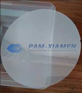
1.S정화의 패턴 사파이어 기판
| 매개 변수 | 명세서 | 단위 |
| 자료 | 고순도 monocrystallinAl2O3 | |
| 직경 | 50.8 ± 0.1 | ㎜ |
| 두께 | 430 ± 10 | ㎛ |
| 총 두께 변화 | ≤10 | ㎛ |
| 기본 플랫 길이 | 16.0 ± 1.0 | ㎜ |
| 기본 평면 방향 | 평면 ± 0.2 | |
| 전면 품질 | Epitaxial 준비 | |
| 뒷면 거칠기 | 1.0 ± 0.1 | ㎛ |
| 표면 방향 A | 0˚off ± 0.1 | |
| 표면 방향 M | 0.2˚off ± 0.10 | |
| 표면 방향 R | R9 | |
| 활 | -10 ~ 0 | ㎛ |
| 경사 | ≤15 | ㎛ |
| 패턴 폭 | 2.7 ± 0.15 | ㎛ |
| 패턴 높이 | 1.7 ± 0.15 | ㎛ |
| 패턴 피치 | 3.0 ± 0.05 | ㎛ |
2.LED 용 패턴 사파이어 기판을 선택하는 이유는 무엇입니까?
On the one hand, the cone-shaped patterned sapphire substrate wafer can effectively reduce the dislocation density of the GaN epitaxial material(the patterned sapphire substrate dislocation is low), thereby reducing the non-radiative recombination of the active area, reducing the reverse leakage current, and improving the life of the LED. On the other hand, the light emitted from the active region is scattered multiple times by the interface of GaN and sapphire substrate, and the exit angle of total reflection light is changed, increasing the probability that the light of the flip-chip LED emerges from the sapphire substrate, thereby improving the extraction efficiency of the light.
요약하면, 나노 패턴 사파이어 기판에서 성장한 LED의 발광 밝기가 기존 LED보다 크게 향상되었습니다. 역 누설 전류가 감소되어 LED의 수명이 연장됩니다.
A patterned sapphire substrate belongs to the semiconductor industry. As a high-brightness epitaxial material, it is the source material of the LED lighting industry. Meanwhile, using PSS Al2O3 wafer to grow epitaxial wafers is the most effective way to improve the brightness of the chip. It is also the best choice for the high-power and high-brightness epitaxial wafers.

자세한 내용은 다음 주소로 이메일을 보내주십시오. victorchan@powerwaywafer.com and powerwaymaterial@gmail.com.