PAM 하문 질화물 코팅 된 실리콘 웨이퍼를 제공합니다.
Stoichiometric LPCVD Nitride on Silicon Wafer Specification
두께 범위 : 100Å - 4500Å
Sides processed: Both
Refractive index: 2.00 +/-.05 @632nm
Film stress: >800MPa Tensile Stress
Wafer size: 1″ -12″inches
Temperature: 800C°
Gases: Dichlorosilane, Ammonia
Equipment: Horizontal vacuum furnace
질화물
LPCVD
PECVD
Stochiometric
Low Stress
Super Low Stress
More specifications of silicon nitride wafer by LPCVD please refer to https://www.powerwaywafer.com/silicon-nitride-wafer-si3n4-thin-film-by-lpcvd.html.
1. About LPCVD
Low-pressure chemical vapor deposition (Low-pressure CVD, LPCVD) is designed to reduce the operating pressure of the reaction gas in the reactor for deposition reaction to below about 133Pa. The LPCVD pressure drops below about 133Pa. Correspondingly, the free path of molecules and the gas diffusion coefficient increase, so that the mass transfer rate of gaseous reactants and by-products is accelerated, and the reaction rate of film formation is increased. When the chip spacing is reduced to 5~10mm, the mass transfer limitation can still be ignored compared with the chemical reaction rate of the chip surface, which creates conditions for vertical densely packed chips, and greatly increases the amount of chips loaded in each batch. The figure below is a schematic diagram of the LPCVD system:
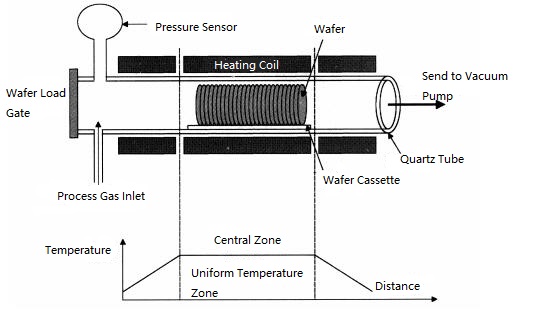
LPCVD Reaction Structure
LPCVD is the mainstream process for film deposition above 90nm. Films deposited by LPCVD will have better step coverage, good composition and structure control, high deposition rate and output. Furthermore, LPCVD does not require carrier gas, thus greatly reducing the source of particle pollution, and is widely used in the high value-added semiconductor industry for thin film deposition. LPCVD is widely used in silicon dioxide (LTO TEOS), silicon nitride (low stress) (Si3N4), polysilicon (LP-POLY), phosphosilicate glass (BSG), borophosphosilicate glass (BPSG), doped polysilicon, graphite alkenes, carbon nanotubes and other thin films.
2. FAQ about Stoichiometric LPCVD Nitride on Silicon Wafers
큐: “Our lab is planning to fabricate some silicon nitride waveguide. so we need to buy some silicon nitride wafers,which means we need around 150 nm stoichiometric silicon nitride films on thermal oxides silicon wafers. the thermal oxide layer should be at least 1 um thickness. silicon substrate is flexible.Below wafer is good thermal oxide wafer for us. Do you have the processing service to grow 150 nm LPCVD low stress silicon nitride on below wafer? Thanks.
Diameter 100mm
Prime grade, SSP
P-type, Dopant B
Orientation<110>
Resistivity 1-10Ωcm
Thickness 500μm
With 1000nm wet thermal Oxide”
A: 100mm P/B <100> 1-10 ohm-cm 500um SSP Prim Grade with 1um of Oxide and 150 nm LPCVD low stress silicon

자세한 내용은 이메일로 문의해 주세요.victorchan@powerwaywafer.com 과 powerwaymaterial@gmail.com.