PAM XIAMEN offers Thinned Silicon Wafers! We have them! In Stock and ready to ship!
Free Standing Thin Silicon Wafers
We offer freestanding super thin silicon wafers with thicknesses ranging from 5µm to 100µm and with diameters from 5mm to 6. The thin Silicon wafers are true mirror finish DSP, good surface flatness, haze-free, void-free, and have low surface RMS (typical 1-2nm) and an ultralow TTV typically less than +/-1µm.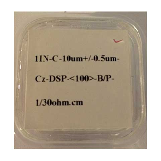
Above Example of Thin Si in Package
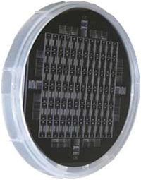
Below are just some of out wafers uses.
Lab-On-Chip ELISA
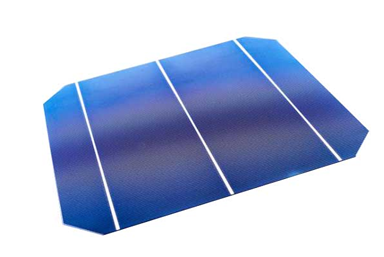
* More efficient Solar Wafers, up to 51%!
* Micro Counter
* Micro-Cantilever Sensing and Actuation Components
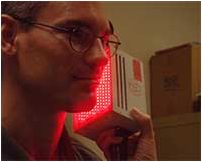
* Photo Dynamic Therapy Laser
* Light Engine for Portable Information Display, and
* Dynamic Diagnostics Tools for Light Emitting Devices
PAM XIAMEN along with our partners now specializes optical MEMS and specialty silicon products. These products and services include
· Deformable mirrors for adaptive optics
· Large format ASIC drivers for deformable mirrors
· MEMS, telecom, instrumentations, and piezoelectrics
· Speciality silicon products such as super thin silicon wafers
· Silicon nitride TEM windows/grids
· PMN-PT/Silicon Unimorphs for optics
· MEMS, measurement, and piezoelectric industries
· Wafer services including bonding, coating, grinding/lapping/polishing, and wafer dicing
Wafer Thicknesses of 5um, 10um, 25um, 50um 100um and more!
We have a large in stock inventory of super-thin Silicon ranging from 5um, 25um, 50um and so on.
Our super-thin silicon production is based on a proprietary combination of the following
· Wafer Bonding
· Lapping
· Polishing
· Debodning Process
Diameter/dimension range from <25.4mm – 150mm, larger is some cases.
The thin wafers are haze and void free. They have low surface roughness of 1-2nm and TTV +/-1um.
Rigid Wafer Ring for Easy Handling
We can also supply an attachement with rigid wafer ring for our thin silicon wafers. This allows for easy handling.
We can also provide the following services on our thin wafers
· 웨이퍼 다이싱
· Silicon wafer lapping and polishing to 5-50um thickness
· Wafer Bonding to mate a cavity wfer with a bare wafer
· PECVD Nitride, LS Nitride, Oxide and LS Oxide on Silicon Including super thin silicon wafers
· Ebeam and thermal evaporation of metal coatings (Ti, Cr, Au, Pt, Pd, Al, Cu, Ag etc) on our wafers including our super-thin wfers
· IC assembly (wafer dicing, die attachment, wire bonding, flip chip bonding)
자세한 내용은 당사 웹사이트를 방문하십시오:https://www.powerwaywafer.com,
send us email at sales@powerwaywafer.com 과 powerwaymaterial@gmail.com
1990년에 설립된 Xiamen Powerway Advanced Material Co., Ltd(PAM-XIAMEN)는 중국 최고의 반도체 재료 제조업체입니다. PAM-XIAMEN은 고급 결정 성장 및 에피택시 기술, 제조 공정, 엔지니어링 기판 및 반도체 장치를 개발합니다. PAM-XIAMEN의 기술은 반도체 웨이퍼의 더 높은 성능과 더 낮은 비용의 제조를 가능하게 합니다.
PAM-XIAMEN은 Ga, Al, In, As 및 P를 기반으로 III-V 실리콘이 도핑된 n형 반도체 재료에 기판 성장 및 에피택시가 있는 1세대 게르마늄 웨이퍼, 2세대 갈륨 비소에서 고급 결정 성장 및 에피택시 기술을 개발합니다. MBE 또는 MOCVD에 의해 3세대로 성장: LED 및 전원 장치 응용 분야를 위한 실리콘 카바이드 및 질화 갈륨.