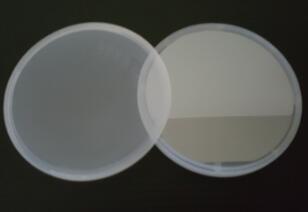
PAM-XIAMEN can offer 780nm laser diode wafer with quantum well based on GaAs substrate. The semiconductor lasers fabricated our LD wafer are applied in the fields of laser cutting, laser coating, laser medical treatment, optical communication, infrared security and etc., which have the disadvantages of high electro-optical conversion efficiency, good spectral purity, small size, and high reliability. The laser diode wafers for 780nm wavelength are for sale as following:

1. Epitaxial Wafer Structures for Laser Diode 780nm
1.1 780nm LD Wafer
780nm LD structures (PAM210625-LD780)
P+ GaAs P>5E19, d=0.15μm
P- AlGaInP and undoped AlGaInP d~1.5μm
Undoped GaInAsP QW PL:765+-10nm
Undoped AlGaInP and N- AlGaInP , d~1.5μm
N GaAs buffer
N GaAs substrate N=(0.4~4)×1018 d=350~625μm (100) 10°off <111>A
1.2 780nm AlGaInP/GaAs Laser Structure Wafer
Xiamen Powerway(PAM-XIAMEN), a leading developer and manufacturer of compound semiconductor epitaxial wafers providing 780nm AlGaInP/GaAs laser structure wafers.
| Layer | Material | X | Y Strain tolerance | PL | Thickness | Type | Level | |
| - | - | - | - | (ppm) | (nm) | (um) | (cm-3) | |
| 8 | GaAs | - | - | - | - | 0.1 | P | >2.00E19 |
| 7 | GaIn(x)P | 0.49 | - | +/-500 | - | 0.05 | P | - |
| 6 | [Al(x)Ga]In(y)P | 0.3 | 0.49 | +/-500 | - | 1 | P | - |
| 5 | GaIn(x)P | 0.49 | - | +/-500 | - | 0.5 | U/D | - |
| 4 | GaAs(x)P | 0.77 | - | - | 770 | U/D | - | |
| 3 | GaIn(x)P | 0.49 | - | +/-500 | 0.5 | U/D | - | |
| 2 | [Al(x)Ga]In(y)P | 0.3 | 0.49 | +/-500 | - | 1 | N | - |
| 1 | GaAs | - | - | - | - | 0.5 | N | - |
| 0 | GaAs substrate | - | - | - | - | - | N | - |
1.3 780 nm Fabry-Perot (FP) Laser Diode (LD) Epi-wafer
The 780 nm Fabry-Perot (FP) laser diode (LD) epi-wafer, designed especially for the high-power characteristics, is grown by metal-organic chemical vapor deposition (MOCVD), with GaAsP quantum well as the active layer
Source:PAM-XIAMEN
2. Technical Features of the 780nm Laser Diode Wafer
The 780nm laser diode wafer manufactured by PAM-XIAMEN has the following technical features:
Epitaxial and wafer process balance uniformity and mass production cost control.Meanwhile, the wavelength uniformity in the laser chip can be controlled within ±1nm by laser diode wafer, and the chip yield rate made from our laser diode wafer is greater than 90%.
Mature material epitaxy technology: MOCVD epitaxy process and MBE epitaxy process can be used together to achieve corrosion stop layer epitaxy, extended waveguide epitaxy, cascade tunnel junction epitaxy, secondary epitaxy, etc., to meet the high quality of GaAs-based laser diode wafer epitaxy.
High-efficiency and high-reliability LD wafer technology: Integrated chip structure design technology based on lase diode wafers and packaging structure enables the laser to have the best electro-optical conversion efficiency at the operating point.
In addition, The wavelength of the LD emission is also related to the thickness of the quantum well. Quantum well materials of different composition and thickness for the laser diode wafer can cover a wide range of light emission. Take the PAM-XIAMEN’s 780nm laser diode wafer for example, to obtain the 780nm wavelength, we use different combinations of composition and thickness. More parameters please see the first point above. This brings great flexibility to the quantum well design of semiconductor lasers.

