InGaP / GaAs heterojunction bipolar transistor (HBT) has become one of the highly competitive and promising high-speed solid-state devices in the current microwave and millimeter wave field due to its high reliability, low cost, and relatively mature technology. PAM-XIAMEN provide InGaP / GaAs HBT wafers. [...]
2023-07-03meta-author
PAM-PA01 series are pixel electrode structured detectors based on CZT crystal. They can detect X-ray, γ-ray and imaging. They have a high energy and space resolution.
1. Specification of CZT High Resolution Pixel Detector
Material
CdZnTe
Density
5.8g/cm3
Volume resistance
>1010Ω.cm
Dimensions
10.0×10.0mm2
Thickness
2.0mm
5.0mm
Pixel size
1.1×1.1mm2
Pixel array
8×8
Electrode material
Au
Operation temperature
-20℃-+40℃
Energy range
20KeV~700MeV
20KeV~700MeV
Energy resolution(22℃)
<6%@59.5KeV
<4.5%@122KeV
<3%@662KeV
Defective pixel(DP)
10℃~40℃
Storage temperture
20%-80%
Remarks
Customized available
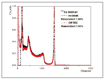
2. Spectrum of [...]
2019-04-24meta-author
PAM XIAMEN offers MgF2 crystal.
MgF2 is an excellent Infrared crystal Crystals. PAM XIAMEN supplies BaF2 crystal substrate, window and blank up to 3″ diameter for all IR applications
Xtl Structure
Lattice (A)
Melting Point
Density g/cm3
Hardness
Thermal Expansion
Refractive index
Tetragonal
a = 4.64
1255 oC
3.18
6 (mohs)
13.7×10⁻⁶ / oC, // c8.48×10-6/ oC, perpen. c
ho 1.37740
c = 3.06
he 1.38945
MgF2 [...]
2019-05-10meta-author
PAM XIAMEN offers 4″ Test Grade Silicon Wafer.
Can you quote the same silicon wafer but 100 wafer instead of 50 Need to be packed in 25 wafer pack with cleanroom paper separators
• 50 silicon wafers (reclaim or test) to serve as polish [...]
2019-06-28meta-author
PAM XIAMEN offers TeO2 Tellurium Dioxide Crystals.
Tellurium Dioxide, TeO2 is an excellent ascousto-optic (AO) crystal with high AO figure of merit, birefringence, good optical rotation and slow propagation velocity along [110] direction. The resolution of AO devices made of TeO2 crystals will increase several [...]
2019-03-15meta-author
Xiamen Powerway Advanced Material Co.,Ltd., a leading supplier of InGaAs (Indium Gallium Arsenide) wafer and other related products and services announced the new availability of size 2″ is on mass production in 2017. This new product represents a natural addition to PAM-XIAMEN’s product line.
Dr. [...]
2017-06-19meta-author