PAM-XIAMEN offers silicon ingot with FZ Intrinsic undoped, MCC lifetime (Minority Charge Carrier Lifetime) more than 1000Ωcm.
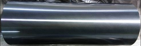
Silicon Ingot, FZ intrinsic undoped, MCC lifetime
An intrinsic(pure) semiconductor, also called an undoped semiconductor or i-type semiconductor,
is a pure semiconductor without any significant dopant species present. The number of charge carriers is therefore determined by the properties of the material itself instead of the amount of impurities.
In intrinsic semiconductors the number of excited electrons and the number of holes are equal: n = p.
This may even be the case after doping the semiconductor, though only if it is doped with both donors and acceptors equally. In this case, n = p still holds, and the semiconductor remains intrinsic, though doped.
1. Specifications of FZ Intrinsic Silicon Ingot
| Crystal# | Diameter (mm) |
Orientation | Lenth (mm) |
Weight (kg) |
Ingot Head Central Resistivity A | Ingot Head Spot Measurement A1 | Ingot Head Spot Measurement A2 | Ingot End Central Resistivity B | Ingot End Spot Measurement B1 | Ingot End Spot Measurement B2 | MCC lifetime A (μs) |
MCC lifetime B (μs) |
| 1806A-929-2-1 | 100 | <111> | 135 | 2.505 | 86000 | 72000 | 65800 | 25000 | 43000 | 30000 | 1020 | 1020 |
| FN100A1801A-621-3 | 100 | <111> | 293 | 5.505 | 32000 | 62000 | 43000 | 33000 | 65000 | 37000 | 1150 | 1150 |
| 1138-4 | 100 | <111> | 152 | 2.830 | 45000 | 96000 | 61000 | 38000 | 85000 | 40000 | 1150 | 1150 |
| 512-1-1-1 | 100 | <111> | 114 | 2.145 | 180000 | 180000 | 180000 | 32000 | 170000 | 145000 | 1020 | 1020 |
2. FAQ about MCC Lifetime Measurement
Q: Please tell me more about your MCC lifetime measurement. How do you measure and guarantee the MCC lifetime?
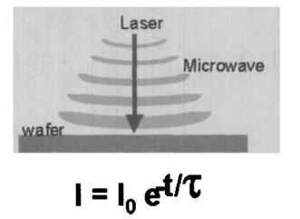
A: Normally, μPCD-microwave photoconductivity decay is used to measure the minority charge carrier lifetime (MCC lifetime) of the wafer quickly, without contact and without damage. Specifically, Using a laser with a wavelength of 904 nm to excite the silicon wafer (for silicon, the implantation depth is about 30 μm), electron hole pairs are generated, resulting in an increase in the conductivity of the sample. When the external light is removed, the conductivity decays exponentially with time.
This trend is indirect. Reflecting the attenuation trend of the minority carrier number, the lifetime of minority carriers (MCC lifetime) can be obtained by microwave(Frequency 10.225GHz) detection of the conductivity of the silicon wafer with time.
Attached schematic diagram of measuring the lifetime of minority materials by microwave photoconductive attenuation method:
3. FAQ about Resistivity Measurement
Q1: deliver 9 points resistivity measurement results for the Si ingot after growth, but after some time, when the resistivity stabilize?
A: After silicon crystal growth, the resistivities of several points would be test when temperature is 23°C, they are stable.
A: After silicon crystal growth, the resistivities of several points would be test when temperature is 23°C, they are stable.
Q2: deliver 5 points resistivity measurement results for the ingot after growth, but after some time, when the resistivity stabilize?
A: After Si crystal growth, the resistivities of several points would be test when temperature is 23°C, they are stable.
A: After Si crystal growth, the resistivities of several points would be test when temperature is 23°C, they are stable.
Q3: deliver dia-scan for resistivity measurement results in, for example, 3mm pitch, 6mm pitch, etc. through the center from the edge of the Si ingot (measured after some time when the resistivity stabilize)?
A: After crystal growth, the resistivities of several points would be test when temperature is 23°C, they are stable.
A: After crystal growth, the resistivities of several points would be test when temperature is 23°C, they are stable.
Q4 explain in how many points you measure resistivity to guarantee the Ro=(10,000-20,000)Ohmcm of silicon ingot?
A: Normally test 5 points resistivity of silicon ingot.
A: Normally test 5 points resistivity of silicon ingot.

For more information, please contact us email at victorchan@powerwaywafer.com and powerwaymaterial@gmail.com.