Measurements on the spectroscopic performance of CdZnTe coplanar grid detectors
A performance study was performed for CdZnTe coplanar grid (CPG) detectors when used as γ-ray spectrometers. The detectors have the crystal volumes of 1, 1.6875 and 2.25 cm3, respectively. Time stability of each CdZnTe CPG detector was investigated in a long-term operation (time span of 0.25 to about 100 h). The spectroscopic performances were measured at different bias voltages and at various photon energies ranging from 59.6 keV (241Am) to 1332.5 keV (60Co) for each detector, and evaluated by using the following parameters: energy resolution in FWHM, peak tailing in peak-to-valley (P/V) ratio and in FWHM/FW.25 M ratio, and photofraction using the acquired γ-ray spectra. No polarization effect was observed in terms of count rate, energy resolution and peak centroid shift. The obtained results indicate that better time stability and excellent spectroscopic performances of the present CdZnTe CPG detectors are shown for a room temperature γ-ray spectroscopy.
Highlights
► The responses of CdZnTe coplanar grid detectors were studied as a room temperature γ-ray spectroscopy.
► The performance data were evaluated by using energy resolution, peak tailing and photofraction parameters.
► Better time stability and excellent spectroscopic performance are shown in high quality CdZnTe materials.

Fig. 1. Time stability of the coplanar grid CdZnTe detectors’ response to various photon energies in terms of photopeak centroid shift.
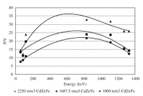
Fig. 2. Variations in peak-to-valley ratios with increasing energy for coplanar grid CdZnTe detectors.
Source: Applied Radiation and Isotopes
If you need more information about Measurements on the spectroscopic performance of CdZnTe coplanar grid detectors, please visit our website:https://www.powerwaywafer.com/, send us email at sales@powerwaywafer.com or powerwaymaterial@gmail.com.