mproved process control, lowered costs and reduced risks through the use of non-destructive mobility and sheet carrier density measurements on GaAs and GaN wafers
Improved process control, lowered costs and reduced risks can be realized through the use of non-destructive mobility and sheet charge density measurements during the fabrication of GaAs and GaN wafers. The results from this microwave-based technique are shown to agree with destructive van der Pauw Hall testing results to within ±5%. In addition, it has the ability to map wafer uniformity and provide separated 2DEG data for thick cap or multi-layered structures. As a result, this technique provides an efficient and cost-effective alternative to current process control metrology methods, while providing the user with important process control data.
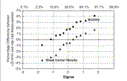
Fig. 1. Comparison of mobility and sheet carrier density measurements for GaAs pHEMT Hall wafers.
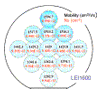
Fig. 2. Mapping of mobility and sheet carrier density for a 2 inch GaN HEMT wafer.
Source: Journal of Crystal Growth
If you need more information about Improved process control, lowered costs and reduced risks through the use of non-destructive mobility and sheet carrier density measurements on GaAs and GaN wafers, please visit our website:https://www.powerwaywafer.com/, send us email at sales@powerwaywafer.com orpowerwaymaterial@gmail.com