The results of GaN epitaxial crystal growth on 4° off-axis Si- and C-face 4H-SiC without buffer layers by tri-halide vapor-phase epitaxy (THVPE) with high-speed wafer rotation and the properties of the obtained material are briefly described in this paper. GaN epitaxial layers were grown [...]
2019-10-18meta-author
The photoluminescent germanium nanocrystals (Ge-NCs) were successfully incorporated into electrospun polymeric nanofiber matrix in order to develop photoluminescent nanofibrous composite web. In the first step, the synthesis of Ge-NCs was achieved by nanosecond pulsed laser ablation of bulk germanium wafer immersed in organic liquid. The size, [...]
Study on the mechanism of using IR illumination to improve the carrier transport performance of CdZnTe detector
Different wavelength IR light (770–1150 nm) was used to evaluate the effect of IR light on the carrier transport performance of CdZnTe detector. The effective mobility-lifetime product (μτ*) [...]
2013-09-27meta-author
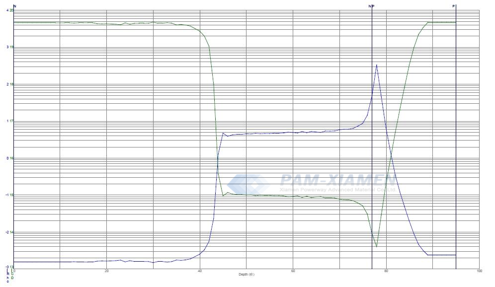
PAM XIAMEN offers 4″ Silicon Wafer.
Material
Orient.
Diam.
Thck
(μm)
Surf.
Resistivity
Ωcm
Comment
p-type Si:B
[100]
4″
400
P/P
0.001-0.005
SEMI Prime
p-type Si:B
[100]
4″
500
P/P
0.001-0.005
SEMI Prime, Wafers with striation marks
p-type Si:B
[100]
4″
525
P/P
0.001-0.005
SEMI Prime, TTV<5μm, Bow<15μm, Warp<30μm
p-type Si:B
[100]
4″
525
P/E
0.001-0.002
SEMI Prime, TTV<4μm
p-type Si:B
[100]
4″
525
P/E
0.001-0.005
SEMI Prime, TTV<5μm
p-type Si:B
[100]
4″
525
BROKEN
0.001-0.005
Broken wafer (shattered into many pieces)
p-type Si:B
[100]
4″
800
C/C
0.001-0.005
SEMI, With striation marks
p-type Si:B
[100]
4″
?
P/P
SEMI Test
p-type Si:B
[100]
4″
375
P/E
<0.0015 {0.00091-0.00099}
SEMI Prime, TTV<3μm
p-type Si:B
[111]
4″
350
P/E
2-3
Prime, NO Flats
p-type Si:B
[111]
4″
1000
P/P
1-10
SEMI Prime, Cassettes of 10 [...]
2019-03-05meta-author
Bulk GaN Crystal Grown by HVPE
We succeeded in preparing very thick c-plane bulk gallium nitride (GaN) crystals grown by hydride vapor phase epitaxy. Growth of the bulk GaN crystals was performed on templates with 3 μm GaN layer grown by metal organic chemical vapor [...]
2012-10-16meta-author
Effects of sample processing on the performance of CdZnTe crystals
Due to the outstanding properties of CdZnTe materials, CdZnTe detectors have been the research focus for X- and gamma ray applications for many years. For CdZnTe detector fabrication heat treatments are often desirable. In order to provide detailed information of the CdZnTe crystal [...]