GaAs ialah bahan semikonduktor celah jalur langsung III-V tipikal dengan sifat optoelektronik yang sangat baik dan mobiliti tinggi, menjadikannya sesuai untuk pengeluaran peranti RF berkelajuan tinggi. GaAs juga boleh membentuk struktur telaga kuantum dengan GaAlAs, meningkatkan lagi prestasi peranti pemancar cahaya (arus ambang rendah, lebar talian sempit). Bahan epitaksi filem nipis GaAs/GaAIAs kini merupakan bahan semikonduktor III-V yang paling banyak digunakan dan dikaji awal, dengan proses dan prestasi matang, sesuai untuk membuat pelbagai jenis peranti fotonik, termasuk peranti aktif dan pasif, dan oleh itu boleh mencapai satu- penyepaduan cip pelbagai peranti fotonik.
PAM-XIAMENboleh menyediakan wafer berasaskan GaAs dengan lapisan AlGaAs ketebalan tersuai untuk mengarang cip bersepadu fotonik(PIC) berasaskan AlGaAs. Ambil contoh struktur epitaxial filem nipis berikut:
1. Epitaksi Filem Nipis AlGaAs / GaAs
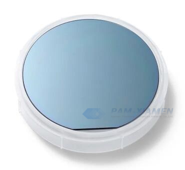
| Wafer Epitaksi GaAs 4” dengan Lapisan AlGaAs (PAM210223-ALGAAS) | ||
| Lapisan No. | Bahan Epi | ketebalan |
| 4 | GaAs | – |
| 3 | Al0.7Ga0.3As | – |
| 2 | Al0.2Ga0.8As | – |
| 1 | Al0.7Ga0.3As | 600nm |
| substrat | GaAs | |
2. Mengenai Cip Bersepadu Fotonik berdasarkan Filem Epitaxial AlGaAs
PIC, juga dikenali sebagai cip fotonik, ialah cip mikro yang merangkumi dua atau lebih komponen fotonik untuk membentuk litar berfungsi.
Penyelidik telah melampirkan filem nipis pemendapan epitaksi AlGaAs pada substrat silikon oksida melalui penyepaduan hetero, dan menggunakan teknologi pemprosesan platform terobosan terkini untuk menyediakan pandu gelombang dengan kontras indeks biasan tinggi sambil mengurangkan kehilangan perambatan pandu gelombang. Akibatnya, kadar sumber cahaya kuantum telah meningkat sebanyak 1,000 kali ganda melalui rongga resonan yang dibentuk oleh pertumbuhan epitaxial filem nipis AlGaAs, dan kecekapannya adalah 1,000 kali lebih tinggi daripada mana-mana teknologi sebelumnya, membolehkan berbilion pasangan foton terjerat dicipta setiap saat daripada pancaran laser mikro-watt, meningkatkan kelajuan pengkomputeran komputer kuantum.
In addition to greatly improving the rate of photon sources, the power consumption required to achieve photon sources based on thin film epitaxy of AlGaAs has also been reduced from 1.4W to 100uW, and the volume has been reduced to smaller than a hair. The advantages of AlGaAs thin film epitaxial heterostructures in integrating laser diodes and other optical devices make it possible to design ultra-small size and highly integrated devices, effectively reducing the size and weight of components to meet practical applications.
Photonic integrated chips fabricated on thin film epitaxy can be used to create faster and more energy efficient devices. This is because thin film crystal epitaxial PICs can sense with the highest accuracy and are very effective in processing and transmitting data. They can also be integrated with traditional electronic chips and applications, covering a range of industries, including data and telecommunications, medical and healthcare, engineering, and transportation.
Remark:
The Chinese government has announced new limits on the exportation of Gallium materials (such as GaAs, GaN, Ga2O3, GaP, InGaAs, and GaSb) and Germanium materials used to make semiconductor chips. Starting from August 1, 2023, exporting these materials is only allowed if we obtains a license from the Chinese Ministry of Commerce. Hope for your understanding and cooperation!

For more information, please contact us email at victorchan@powerwaywafer.com and powerwaymaterial@gmail.com.