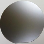

wafer InP
PAM-XIAMEN offers VGF InP(Indium Phosphide) wafer with prime or test grade including low dope, N type or semi-insulating. The mobility of InP wafer is different in different type, low doped one>=3000cm2/V.s, N type>1000 or 2000cm2V.s(depends on different doping concentration), P type: 60+/-10 or 80+/-10cm2/V.s(depends on different Zn doping concentration), and semi-insulting one>2000cm2/V.s, the EPD of Indium Phosphide is below 500/cm2 normally.
- Penerangan
Penerangan Produk
wafer InP
PAM-XIAMEN, a leading InP wafer supplier, offers Compound Semiconductor InP wafer – Indium Phosphide which are grown by LEC(Liquid Encapsulated Czochralski) or VGF(Vertical Gradient Freeze) as epi-ready or mechanical grade with n type, p type or semi-insulating. The InP wafer orientation (111) or (100) is available. And the dopants can be Sulphur, Sn(Tin), Zinc or customs. The Laser Mark as specified on backside of InP wafer along with primary flat. The orientation with slight deflection angle is available, such as (100)0.075° towards [110]]±0.025°.
Indium phosphide (InP) is a binary semiconductor composed of indium and phosphorus. It has a face-centered cubic (“zinc blende”) crystal structure, identical to that of GaAs and most of the III-V semiconductors. Indium phosphide can be prepared from the reaction of white phosphorus and indium iodide [clarification needed] at 400 °C., also by direct combination of the purified elements at high temperature and pressure, or by thermal decomposition of a mixture of a trialkyl indium compound and phosphide. Indium phosphide wafers are used in high-power and high-frequency electronics [citation needed] because of the superior electron velocity with respect to the more common semiconductors silicon and gallium arsenide. The InP wafer size we can offer is 2”, 3” and 4”, and the InP wafer thickness will be 350~625um.
Berikut adalah spesifikasi terperinci:
| Item | Specifications | |||
| Dopant | N-type | N-type | P-type | SI-type |
| Conduction Type | low doped | Sulphur | Zinc | lron |
| Wafer Diameter | 2″ | |||
| Wafer Orientation | (100)±0.5° | |||
| Wafer Thickness | Min:325 Max:375 | |||
| Primary Flat Length | 16±2mm | |||
| Secondary Flat Length | 8±1mm | |||
| Carrier Concentration | 3×1016cm-3 | (0.8-6)x1018cm-3 | (0.6-6)x1018cm-3 | N/A |
| Mobility | (3.5-4)x103cm2/V.s | (1.5-3.5)x103cm2/V.s | 50-70×103cm2/V.s | >1000cm2/V.s |
| Resistivity | N/A | N/A | N/A | N/A |
| EPD | <1000cm-2 | <500cm-2 | <1×103cm-2 | <5×103cm-2 |
| TTV | <10um | |||
| BOW | <10um | |||
| WARP | <12um | |||
| Laser marking | upon request | |||
| Suface finish | P/E, P/P | |||
| Epi ready | yes | |||
| Package | Single wafer container or cassette | |||
2″ P Type InP Wafer Specification
| Item | Parameter | UOM |
| Material | InP | |
| Conduct Type/Dopant | S-C-P/Zn | |
| Grade | Prime | |
| Diameter: | 50.5±0.4 | mm |
| Orientation: | (100)±0.5° | |
| Orientation Angle: | / | |
| Thickness: | Min:325 Max:375 | um |
| Carrier Concentration: | Min:0.6E18 Max:3E18 | cm-3 |
| Resistivity: | Min:/ Max:/ | ohm.cm |
| Mobility: | Min:/ Max:/ | cm-2/V.sec |
| EPD: | Ave<:1000 Max<:/ | cm-2 |
| TTV: | Max:10 | um |
| TIR: | Max:10 | um |
| BOW: | Max:10 | um |
| Warp: | Max:15 | um |
| Flat Option: | EJ | |
| Primary Flat Orientation: | (0-1-1) | |
| Primary Flat Length: | 16±1 | mm |
| Secondary Flat Orientation: | (0-11) | |
| Secondary Flat Length: | 7±1 | mm |
| Suface: | Side 1:Polished Side 2:etched | |
| Edge Rounding | 0.25(Conform to SEMI Standards) | mmR |
| Particle Count: | / | |
| Package | individual container filled with N2 | |
| Epi-ready | Yes | |
| Laser Marking | Back side major flat | |
| Remark: | Special specifications will be discussed separately | |
3″ InP Wafer Specification
| Item | Specifications | |||
| Dopant | N-type | N-type | P-type | SI-type |
| Conduction Type | low doped | Sulphur | Zinc | lron |
| Wafer Diameter | 3″ | |||
| Wafer Orientation | (100)±0.5° | |||
| Wafer Thickness | 600±25um | |||
| Primary Flat Length | 16±2mm | |||
| Secondary Flat Length | 8±1mm | |||
| Carrier Concentration | ≤3×1016cm-3 | (0.8-6)x1018cm-3 | (0.6-6)x1018cm-3 | N/A |
| Mobility | (3.5-4)x103cm2/V.s | (1.5-3.5)x103cm2/V.s | 50-70×103cm2/V.s | >1000cm2/V.s |
| Resistivity | N/A | N/A | N/A | N/A |
| EPD | <1000cm-2 | <500cm-2 | <1×103cm-2 | <5×103cm-2 |
| TTV | <12um | |||
| BOW | <12um | |||
| WARP | <15um | |||
| Laser marking | upon request | |||
| Suface finish | P/E, P/P | |||
| Epi ready | yes | |||
| Package | Single wafer container or cassette | |||
4″ InP Wafer Specification
| Item | Specifications | |||
| Dopant | N-type | N-type | P-type | SI-type |
| Conduction Type | low doped | Sulphur | Zinc | lron |
| Wafer Diameter | 4″ | |||
| Wafer Orientation | (100)±0.5° | |||
| Wafer Thickness | 600±25um | |||
| Primary Flat Length | 16±2mm | |||
| Secondary Flat Length | 8±1mm | |||
| Carrier Concentration | ≤3×1016cm-3 | (0.8-6)x1018cm-3 | (0.6-6)x1018cm-3 | N/A |
| Mobility | (3.5-4)x103cm2/V.s | (1.5-3.5)x103cm2/V.s | 50-70×103cm2/V.s | >1000cm2/V.s |
| Resistivity | N/A | N/A | N/A | N/A |
| EPD | <1000cm-2 | <500cm-2 | <1×103cm-2 | <5×103cm-2 |
| TTV | <15um | |||
| BOW | <15um | |||
| WARP | <15um | |||
| Laser marking | upon request | |||
| Suface finish | P/E, P/P | |||
| Epi ready | yes | |||
| Package | Single wafer container or cassette | |||
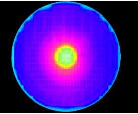
PL(Photoluminescence) Test of indium phosphide Wafer
We measure InP wafers by Peak Lambda, Peak int, and FWHM, the spectra mapping is as follows:

About InP Wafer Application
As a new type of compound semiconductor material, InP wafer market share is increasing gradually. Due to the excellent indium phosphide properties, the performance of microwave power source devices, microwave amplifiers and gate FETs fabricated on InP material will be better than those fabricated on existing gallium arsenide materials. Indium phosphide heterojunction lasers are also extremely promising light sources in optical fiber communications.
InP wafer fabrication for devices, like growing millimeter wave microelectronic devices and optoelectronic device materials for optical fiber communications, is widely used. With the continuous improvement of device performance and the reduction of device size, the quality requirements for indium phosphide wafers are getting higher and higher. Therefore, the InP wafer process is optimizing gradually.
The the typical values is see below data:
| Peak Lambda(nm) | Peak Int | FWHM(nm) |
| 1279.4 | 7.799 | 48.5 |
| 1279.8 | 5.236 | 44.6 |
Awak juga mungkin menyukai…
-
SiC Epitaxy
Kami menyediakan filem adat nipis (silikon karbida) SiC epitaxy pada 6H atau 4H substrat untuk pembangunan peranti silikon karbida. SiC epi wafer digunakan terutamanya untuk diod Schottky, logam-oksida semikonduktor bidang kesan transistor, kesan medan simpang -
wafer Inas
PAM-XIAMEN offers Compound Semiconductor InAs wafer – indium arsenide wafer which are grown by LEC(Liquid Encapsulated Czochralski) as epi-ready or mechanical grade with n type, p type or semi-insulating in different orientation(111) or (100). In addition, InAs single crystal has high electron mobility and is an ideal material for making Hall devices.
-
Freestanding Gan substrat
PAM-XIAMEN telah menubuhkan teknologi pembuatan untuk berdiri sendiri (galium nitrida) wafer Gan substrat, yang adalah untuk UHB-LED dan LD. Berkembang dengan teknologi hidrida fasa wap epitaxy (HVPE), substrat Gan kami mempunyai ketumpatan kecacatan rendah.
-
GASB Wafer
PAM-XIAMEN offers Compound Semiconductor GaSb wafer – gallium antimonide which are grown by LEC(Liquid Encapsulated Czochralski) as epi-ready or mechanical grade with n type, p type or semi-insulating in different orientation(111) or (100).
-
GaP Wafer – Can’t Offer Temporarily
PAM-XIAMEN offers Compound Semiconductor GaP wafer – gallium phosphide wafer which is grown by LEC(Liquid Encapsulated Czochralski) as epi-ready or mechanical grade with n type, p type or semi-insulating in different orientation(111)or(100). -
Ge (Germanium) kristal tunggal dan Wafers
PAM-XIAMEN offers 2”, 3”, 4” and 6” germanium wafer, which is short for Ge wafer grown by VGF / LEC. Lightly doped P and N type Germanium wafer can be also used for Hall effect experiment. At room temperature, crystalline germanium is brittle and has little plasticity. Germanium has semiconductor properties. High-purity germanium is doped with trivalent elements (such as indium, gallium, boron) to obtain P-type germanium semiconductors; and pentavalent elements (such as antimony, arsenic, and phosphorus) are doped to obtain N-type germanium semiconductors. Germanium has good semiconductor properties, such as high electron mobility and high hole mobility. -
GaAs (galium arsenida) Wafers
As a leading GaAs substrate supplier, PAM-XIAMEN manufactures Epi-ready GaAs(Gallium Arsenide) Wafer Substrate including semi-conducting n type, semi-conductor C doped and p type with prime grade and dummy grade. The GaAs substrate resistivity depends on dopants, Si doped or Zn doped is (0.001~0.009) ohm.cm, C doped one is >=1E7 ohm.cm. The GaAs wafer crystal orientation should be (100) and (111). For (100) orientation, it can be 2°/6°/15° off. The EPD of GaAs wafer normally is <5000/cm2 for LED or <500/cm2 for LD or microelectronics.
-
wafer INSB
PAM-XIAMEN offers Compound Semiconductor InSb wafer – Indium antimonide wafer which is grown by LEC(Liquid Encapsulated Czochralski) as epi-ready or mechanical grade with n type, p type or semi-insulating in different orientation(111) or (100). Indium antimonide doped with isoelectronic(such as N doping) can reduce the defect density during the indium antimonide thin films manufacturing process.