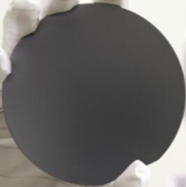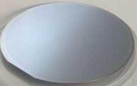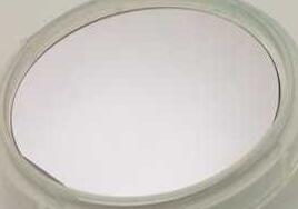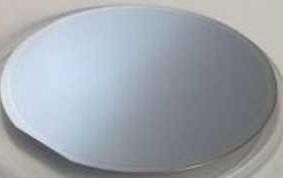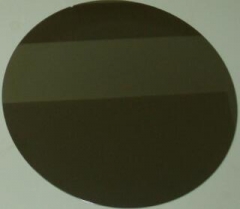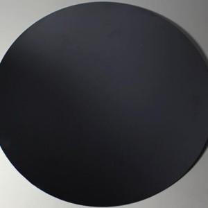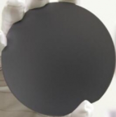
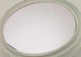
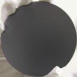
InSb wafer
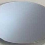

PAM-Xiamen menawarkan kompaun semikonduktor Insb Wafer-Wafer antimonida indium yang ditanam oleh LEC (czochralski cecair yang terkandung cecair) sebagai gred epi-siap atau mekanikal dengan jenis N, jenis P atau separuh insulasi dalam orientasi yang berbeza (111) atau (100). Indium antimonida yang doped dengan isoelektronik (seperti d doping) dapat mengurangkan ketumpatan kecacatan semasa proses pembuatan filem nipis antimonida indium.
- Description
Penerangan
Pam-Xiamen menawarkan kompaun semikonduktor insb wafer-Indium antimonidaWafer yang ditanam oleh LEC (czochralski yang terkandung cecair) sebagai gred epi-siap atau mekanikal dengan jenis N, jenis P atau separuh penebat dalam orientasi yang berbeza (111) atau (100). Indium antimonida yang doped dengan isoelektronik (seperti d doping) dapat mengurangkan ketumpatan kecacatan semasa proses pembuatan filem nipis antimonida indium.
Indium antimonida (INSB) adalah sebatian kristal yang diperbuat daripada unsur -unsur indium (IN) dan antimoni (SB). Ia adalah bahan semikonduktor sempit dari kumpulan III-V yang digunakan dalam pengesan inframerah, termasuk kamera pengimejan haba, sistem FLIR, sistem bimbingan peluru berpandu inframerah, dan dalam astronomi inframerah. Pengesan antimonida indium sensitif antara panjang gelombang 1-5 μm. Indium antimonida adalah pengesan yang sangat biasa dalam sistem pengimejan haba yang diimbas secara mekanikal secara mekanikal. Permohonan lain adalah sebagai sumber radiasi terahertz kerana ia adalah pemancar foto yang kuat.
| Spesifikasi Wafer | |
| Perkara | Spesifikasi |
| Diameter Wafer | 2″50.5±0.5mm |
| 3″76.2±0.4mm | |
| 4″1000.0±0.5mm | |
| Orientasi Kristal | 2″(111)AorB±0.1° |
| 3″(111)AorB±0.1° | |
| 4″(111)AorB±0.1° | |
| ketebalan | 2″625±25um |
| 3″ 800atau900±25um | |
| 4″1000±25um | |
| Panjang rata utama | 2″16±2mm |
| 3″22±2mm | |
| 4″32.5±2.5mm | |
| Panjang rata sekunder | 2″8±1mm |
| 3″11±1mm | |
| 4″18±1mm | |
| Kemasan Permukaan | P/E, P/P |
| Pakej | Epi-siap, bekas wafer tunggal atau kaset CF |
| Spesifikasi elektrik dan doping | |||||
| Jenis Pengaliran | n-jenis | n-jenis | n-jenis | n-jenis | p-type |
| Dopant | doped rendah | Tellurium | Low tellurium | High tellurium | Genmanium |
| EPD cm-2 | 2″3″4″≤50 | 2″≤100 | |||
| Mobility cm² V-1s-1 | ≥4*105 | ≥2.5*104 | ≥2.5*105 | Not Specified | 8000-4000 |
| Carrier Concentration cm-3 | 5*1013-3*1014 | (1-7)*1017 | 4*1014-2*1015 | ≥1*1018 | 5*1014-3*1015 |
.png)
1)2″(50.8mm)InSb Wafer
Orientation:(100)
Type/Dopant:N/low doped
Diameter:50.8mm
Thickness:300±25µm;500um
Nc:<2E14a/cm3
Polish:SSP
2)2″(50.8mm)InSb Wafer
Orientation:(100)
Type/Dopant:N/Te
Diameter:50.8mm
Carrier Concentration: 0.8 – 2.1 x 1015 cm-3
Thickness:450+/- 25 um;525±25µm
EPD < 200 cm-2
Polish:SSP
3)2″(50.8mm)InSb Substrate
Orientation:(111) + 0.5°
Thickness:450+/- 50 um
Type/Dopant:N/low doped
Carrier Concentration: < 5 x 10^14 cm-3
EPD < 5 x 103 cm-2
Surface roughness: < 15 A
Bow/Warp: < 30 um
Polish:SSP
4)2″(50.8mm)InSb Substrate
Orientation:(111) + 0.5°
Type/Dopant:P/Ge
Polish:SSP
5)2″(50.8mm)Indium Antimonide Wafer
Thickness:525±25µm,
Orientation:[111A]±0.5°
Type/Dopant:N/Te
Ro=(0.020-0.028)Ohmcm,
Nc=(4-8)E14cm-3/cc,
u=(4.05E5-4.33E5)cm²/Vs,
EPD<100/cm²,
Mobility:>1E4cm2/Vs
One side edge;
In(A) Face: Chemically-mechanically final polished to 0.1µm (Final Polish),
Sb(B) Face: Chemically-mechanically final polished to <5µm (Lasermark),
NOTE: Nc and Mobility are at 77ºK.
Polish:SSP;DSP
6)2″(50.8mm) GaSb
Thickness:525±25µm,
Orientation:[111B]±0.5°,
Type/Dopant:P/low doped;N/low doped
Polish:SSP;DSP
Surface Condition and other Specification
Indium Antimonide wafer can be offered as wafers with as-cut, etched or polished finishes with wide range of doping concentration and thickness. The InSb wafer could be high quality epi-ready finishing.
Orientation Specification
Indium antimonide surface orientations are supplied to an accuracy of +/- 0.5 degrees using a triple axis X-Ray diffractometer system. Indium antimonide substrates can also be supplied with very precise misorientations in any direction from the growth plane. The available InSb wafer orientation could be (100),(111), (110) or other orientation or mis degree.
Packaging condition
Polished wafer: individually sealed in two outer bags in inert atmosphere. Cassette shipments are available if required.
As-cut Wafer: Cassette shipment. (Glassine bag available on request).
Indium Antimonide Properties and Uses
The indium antimonide crystal structure is silver, brittle, and zinc blende structure. The indium antimonide lattice constant is 6.48 Å, and indium antimonide is a direct bandgap material with a narrow band gap of 0.18 eV. The indium antimonide conduction electron mobility is as high as 7800 cm2/V·s , which can be used to make infrared detectors, photomagnetic detectors and Hall devices.
* Export license required: single crystal InSb with EPD <50/cm-2