
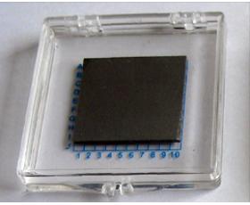
GaAs Epiwafer
PAM-XIAMEN is manufacturing various types of epi wafer III-V silicon doped n-type semiconductor materials based on Ga, Al, In, As and P grown by MBE or MOCVD. We supply custom GaAs epiwafer structures to meet customer specifications, please contact us for more information.
- Penerangan
Penerangan Produk
GaAs Epi wafer
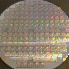
As a leading GaAs epi wafer foundry, PAM-XIAMEN are manufacturing various types of epiwafer III-V silicon doped n-type semiconductor materials based on Ga, Al, In, As and P grown by MBE or MOCVD, which make a low gallium arsenide epi wafer defect. We supply custom GaAs epiwafer structures to meet customer specifications, please contact us for more information.
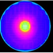
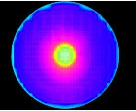
We have numbers of the United States Veeco’s GEN2000, GEN200 large-scale production of epitaxial equipment production line, full set of XRD; PL-Mapping; Surfacescan, and other world-class analysis and testing equipment. The company has more than 12,000 square meters of supporting plant, including world class super-clean semiconductor and a related research and development of the younger generation of clean laboratory facilities.
Specification for all new and featured products of MBE III-V compound semiconductor epitaxial wafer:
| substrat bahan | Keupayaan bahan | Permohonan |
| GaAs | GaAs suhu rendah | THz |
| GaAs | GaAs / GaAlAs / GaAs / GaAs | Schottky Diod |
| Dalam p | InGaAs | pengesan PIN |
| Dalam p | InP / InP / InGaAsP / InP / InGaAs | laser |
| GaAs | GaAs / ALAS / GaAs | |
| Dalam p | InP / InAsP / InGaAs / InAsP | |
| GaAs | GaAs / InGaAsN / AlGaAs | |
| / GaAs / AlGaAs | ||
| Dalam p | InP / InGaAs / InP | photodetectors |
| Dalam p | InP / InGaAs / InP | |
| Dalam p | InP / InGaAs | |
| GaAs | GaAs / InGaP / GaAs / AlInP | Cell solar |
| / InGaP / AlInP / InGaP / AlInP | ||
| GaAs | GaAs / GaInP / GaInAs / GaAs / AlGaAs / GalnP / GalnAs | Cell solar |
| / GalnP / GaAs / AlGaAs / AllnP / GalnP / AllnP / GalnAs | ||
| Dalam p | InP / GaInP | |
| GaAs | GaAs / AlInP | |
| GaAs | GaAs / AlGaAs / GalnP / AlGaAs / GaAs | 703nm Laser |
| GaAs | GaAs / AlGaAs / GaAs | |
| GaAs | GaAs / AlGaAs / GaAs / AlGaAs / GaAs | HEMT |
| GaAs | GaAs / ALAS / GaAs / ALAS / GaAs | mHEMT |
| GaAs | GaAs / DBR / AlGaInP / MQW / AlGaInP / Jurang | wafer LED, lampu keadaan pepejal |
| GaAs | GaAs / GalnP / AlGaInP / GaInP | 635nm, 660nm, 808nm, 780nm, 785nm, |
| / GaAsP / GaAs / GaAs substrat | 950nm, 1300nm, 1550nm Laser | |
| GASB | AlSb / GaInSb / Inas | pengesan IR, PIN, sensing, cemera IR |
| silikon | InP atau GaAs di Silicon | IC kelajuan tinggi / mikropemproses |
| INSB | Berilium didopkan INSB | |
| / Undoped INSB / Te didopkan INSB / |
Gallium arsenide is currently one of the most important compound semiconductor materials with the highest mature epi wafer technology. GaAs material has the characteristics of large forbidden band width, high electron mobility, direct band gap, high luminous efficiency. Due to all all these epi wafer advantages, GaAs epitaxy is currently the most important material used in the field of optoelectronics. Meanwhile, it is also an important microelectronic material. According to the difference in electrical conductivity, GaAs epi wafer materials can be divided into semi-insulating (SI) GaAs and semiconductor (SC) GaAs.
In the field of epitaxial wafers, the epi wafer market share of RF and laser applications is very large.
Untuk lebih spesifikasi terperinci, sila semak perkara berikut:
LT-GaAs epi lapisan pada GaAs substrat
LT GaAs Thin Film for Photodetectors and Photomixers
GaAs Schottky Diod Epitaxial Wafers
InGaAsP / InGaAs pada substrat InP
InGaAs APD Wafers with High Performance
InGaAsN epitaxially pada GaAs atau wafer InP
Struktur bagi photodetectors InGaAs
AlGaP / GaAs Epi Wafer untuk your Solar
sel-sel solar tiga persimpangan
Solar Cell Structure Epitaxially Grown on InP Wafer
Growth of GaAsSb / InGaAs Type-II Superlattice
AlGaAs / GaAs PIN Epitaxial Wafer
1550nm GaInAsP / InP PIN Photodiode Structure
GaAs / AlGaAs / GaAs epi wafer
Sekarang kita senaraikan beberapa spesifikasi:
| GaAs HEMT epiwafer, size:2~6inch | ||
| Perkara | spesifikasi | Catatan |
| parameter | Al komposisi / Dalam komposisi / rintangan Lembaran | Sila hubungi jabatan teknikal kami |
| Dewan mobiliti / 2DEG Konsentrasi | ||
| teknologi pengukuran | X-ray pembelauan / Eddy semasa | Sila hubungi jabatan teknikal kami |
| Dewan Un-kenalan | ||
| injap biasa | Struture bergantung | Sila hubungi jabatan teknikal kami |
| 5000 ~ 6500cm2 / V · S / 0.5 ~ 1.0x 1012cm-2 | ||
| toleransi yang standard | ± 0.01 / ± 3% / tiada | Sila hubungi jabatan teknikal kami |
| GaAs (galium arsenida) pHEMT epiwafer, size:2~6inch | ||
| Perkara | spesifikasi | Catatan |
| parameter | Al komposisi / Dalam komposisi / rintangan Lembaran | Sila hubungi jabatan teknikal kami |
| Dewan mobiliti / 2DEG Konsentrasi | ||
| teknologi pengukuran | X-ray pembelauan / Eddy semasa | Sila hubungi jabatan teknikal kami |
| Dewan Un-kenalan | ||
| injap biasa | Struture bergantung | Sila hubungi jabatan teknikal kami |
| 5000 ~ 6800cm2 / V · S / 2.0 ~ 3.4x 1012cm-2 | ||
| toleransi yang standard | ± 0.01 / ± 3% / tiada | Sila hubungi jabatan teknikal kami |
| Remark:GaAs pHEMT: Compared with GaAs HEMT, GaAs PHEMT also incorporates InxGa1-xAs,where InxAs is constrained to x < 0.3 for GaAs-based devices. Structures grown with the same lattice constant as HEMT, but different band gaps are simply referred to as lattice-matched HEMTs. | ||
| GaAs mHEMT epiwafer, size:2~6inch | ||
| Perkara | spesifikasi | Catatan |
| parameter | Rintangan komposisi / lembaran | Sila hubungi jabatan teknikal kami |
| Dewan mobiliti / 2DEG Konsentrasi | ||
| teknologi pengukuran | X-ray pembelauan / Eddy semasa | Sila hubungi jabatan teknikal kami |
| Dewan Un-kenalan | ||
| injap biasa | Struture bergantung | Sila hubungi jabatan teknikal kami |
| 8000~10000cm2/V ·S/2.0~3.6x 1012cm-2 | ||
| toleransi yang standard | ± 3% / tiada | Sila hubungi jabatan teknikal kami |
| InP HEMT epiwafer, size:2~4inch | ||
| Perkara | spesifikasi | Catatan |
| parameter | Rintangan komposisi / lembaran / Dewan mobiliti | Sila hubungi jabatan teknikal kami |
Remark: GaAs(Gallium arsenide) is a compound semiconductor material,a mixture of two elements, gallium (Ga) and arsenic (As). The uses of Gallium arsenide are varied and include being used in LED/LD, field-effect transistors (FETs), and integrated circuits (ICs)
aplikasi peranti
RF Switch, Power and low-noise amplifiers, Hall sensor, modulator optik
stesen telefon bimbit atau asas: Wireless
Automotive radar, MMIC, RFIC, Fiber optik Communications
GaAs Epi Wafer untuk LED serie / IR:
Huraian 1.General:
1.1 Kaedah Pertumbuhan: MOCVD
1.2 GaAs epi wafer for Wireless Networking
1.3wafer GaAs epi bagi LED/ IR dan LD / PD
2.Epi ciri-ciri komputer wafer:
2.1 Saiz Wafer: 2 "diameter
2.2 GaAs Epi Wafer Structure(from top to bottom):
P + GaAs
p-Jurang
p-AlGaInP
MQW-AlGaInP
n-AlGaInP
DBR n-ALGaAs / AlAs
Buffer
GaAs substrat
3.Chip sepcification (Base pada 9mil * cip 9mil)
3.1 Parameter
Chip Saiz 9mil * 9mil
Ketebalan 190 ± 10um
diameter elektrod 90um ± 5um
3.2 aksara optik elctric (Ir = 20mA, 22 ℃)
Panjang gelombang 620 ~ 625nm
voltan hadapan 1.9 ~ 2.2V
Reverse ≥10v voltan
Reverse 0-1uA semasa
3.3 Light aksara intensiti (Ir = 20mA, 22 ℃)
IV (MCD) 80-140
3.4 Epiwafer avelength
|
Perkara |
Unit |
Merah |
Kuning |
Kuning hijau |
Penerangan |
|
Gelombang Panjang (λD) |
nm |
585.615.620 ~ 630 |
587 ~ 592 |
568 ~ 573 |
IF = 20mA |
Kaedah pertumbuhan: MOCVD, MBE
epitaxy = pertumbuhan filem dengan hubungan yang kristalografi antara filem dan substrat homoepitaxy (autoepitaxy, isoepitaxy) = filem dan substrat adalah bahan yang sama heteroepitaxy = filem dan substrat adalah bahan-bahan yang berbeza. untukmaklumat lanjut kaedah pertumbuhan, sila klik berikut:https://www.powerwaywafer.com/technology.html
Remark:
The Chinese government has announced new limits on the exportation of Gallium materials (such as GaAs, GaN, Ga2O3, GaP, InGaAs, and GaSb) and Germanium materials used to make semiconductor chips. Starting from August 1, 2023, exporting these materials is only allowed if we obtains a license from the Chinese Ministry of Commerce. Hope for your understanding and cooperation!
InGaAs Epitaxy Sensor / Detector:
Shortwave Infrared InGaAs Sensor
InGaAs/InAlAs Epistucture for Single Photon Detector
Epiwafer for Photonic Integrated Chip:
Awak juga mungkin menyukai…
-
wafer InP
PAM-XIAMEN offers VGF InP(Indium Phosphide) wafer with prime or test grade including low dope, N type or semi-insulating. The mobility of InP wafer is different in different type, low doped one>=3000cm2/V.s, N type>1000 or 2000cm2V.s(depends on different doping concentration), P type: 60+/-10 or 80+/-10cm2/V.s(depends on different Zn doping concentration), and semi-insulting one>2000cm2/V.s, the EPD of Indium Phosphide is below 500/cm2 normally.
-
Freestanding Gan substrat
PAM-XIAMEN telah menubuhkan teknologi pembuatan untuk berdiri sendiri (galium nitrida) wafer Gan substrat, yang adalah untuk UHB-LED dan LD. Berkembang dengan teknologi hidrida fasa wap epitaxy (HVPE), substrat Gan kami mempunyai ketumpatan kecacatan rendah.
-
CdZnTe (CZT) Wafer
Kadmium Zinc Telluride (CdZnTe atau CZT) adalah semikonduktor baru, yang membolehkan untuk menukar sinaran elektron dengan berkesan, ia adalah terutamanya digunakan dalam inframerah filem nipis epitaxy substrat, pengesan X-ray dan pengesan Gamma-ray CdZnTe. -
Terapung-Zone Mono-Kristal Silicon
PAM-XIAMEN boleh menawarkan wafer silikon zon terapung, yang diperoleh melalui kaedah Zon Terapung. Rod silikon monohablur diperolehi melalui pertumbuhan zon terapung, dan kemudian memproses rod silikon monohablur menjadi wafer silikon, dipanggil wafer silikon zon terapung. Oleh kerana wafer silikon cair zon tidak bersentuhan dengan pijar kuarza semasa proses silikon zon terapung, bahan silikon berada dalam keadaan terampai. Oleh itu, ia kurang tercemar semasa proses lebur zon terapung silikon. Kandungan karbon dan kandungan oksigen lebih rendah, kekotoran kurang, dan kerintangan lebih tinggi. Ia sesuai untuk pembuatan peranti kuasa dan peranti elektronik voltan tinggi tertentu.
-
Fotoresist Nanofabrikasi
PAM-XIAMEN Tawaran plat photoresist dengan photoresist
-
GaAs (galium arsenida) Wafers
As a leading GaAs substrate supplier, PAM-XIAMEN manufactures Epi-ready GaAs(Gallium Arsenide) Wafer Substrate including semi-conducting n type, semi-conductor C doped and p type with prime grade and dummy grade. The GaAs substrate resistivity depends on dopants, Si doped or Zn doped is (0.001~0.009) ohm.cm, C doped one is >=1E7 ohm.cm. The GaAs wafer crystal orientation should be (100) and (111). For (100) orientation, it can be 2°/6°/15° off. The EPD of GaAs wafer normally is <5000/cm2 for LED or <500/cm2 for LD or microelectronics.
-
SiC Wafer Substrat
Syarikat itu mempunyai barisan pengeluaran substrat wafer SiC(silikon karbida) lengkap yang menyepadukan pertumbuhan kristal, pemprosesan kristal, pemprosesan wafer, penggilap, pembersihan dan ujian. Pada masa kini kami membekalkan wafer SiC 4H dan 6H komersial dengan separa penebat dan kekonduksian dalam paksi atas atau luar paksi, saiz tersedia: 5x5mm2,10x10mm2, 2”,3”,4”, 6” dan 8″, menembusi teknologi utama seperti sebagai penindasan kecacatan, pemprosesan kristal benih dan pertumbuhan pesat, menggalakkan penyelidikan dan pembangunan asas berkaitan epitaksi silikon karbida, peranti, dsb.
-
Ge (Germanium) kristal tunggal dan Wafers
PAM-XIAMEN menawarkan 2”, 3”, 4” dan 6” wafer germanium, yang merupakan singkatan kepada wafer Ge yang ditanam oleh VGF / LEC. Wafer Germanium jenis P dan N yang didop ringan boleh juga digunakan untuk eksperimen kesan Hall. Pada suhu bilik, germanium kristal rapuh dan mempunyai keplastikan yang sedikit. Germanium mempunyai sifat semikonduktor. germanium ketulenan tinggi didopkan dengan unsur trivalen (seperti indium, galium, boron) untuk mendapatkan semikonduktor germanium jenis P; dan unsur pentavalen (seperti antimoni, arsenik, dan fosforus) didopkan untuk mendapatkan semikonduktor germanium jenis N. Germanium mempunyai sifat semikonduktor yang baik, seperti mobiliti elektron tinggi dan mobiliti lubang tinggi.


Produk Berkaitan
-
Gan berasaskan LED Epitaxial Wafer
Gan PAM-XIAMEN-kanak (galium nitrida) berasaskan LED wafer epitaxial adalah untuk tinggi kecerahan diod ultra biru dan hijau pemancar cahaya (LED) dan diod laser (LD) permohonan.
