Gan HEMT Epitaxial Wafer
Gallium Nitride (GaN) HEMTs (High Electron Mobility Transistors) are the next generation of RF power transistor technology. Thanks to GaN technology, PAM-XIAMEN now offer AlGaN/GaN HEMT Epi Wafer on sapphire or Silicon, and AlGaN/GaN on sapphire template.
- Penerangan
Penerangan Produk
GaN HEMT epitaxial wafer is a multilayer film grown epitaxially on a substrate, which usually includes a nucleation layer, a transition layer, a buffer layer, a channel layer, a barrier layer, a cap layer, and a passivation layer from bottom to top. The nucleation layer, like AlGaN or AlN, is used to prevent the substrate material from diffusing into the GaN epitaxial layer. The transition layer may contain hierarchical AlGaN, AlN/GaN superlattice or multilayer AlN to balance the stress between the GaN and the substrate. The higher the Al content in the barrier layer of AlGaN, the higher the 2DEG concentration at the heterojunction. Meanwhile, the lower the threshold voltage of the device, and the higher the current capacity. As the Al ratio increasing, the degree of heterogeneous crystal lattice mismatch will be higher, resulting in a decrease in gallium nitride HEMT electron mobility and a decrease in current capacity.
The High Electron Mobility Transistor (HEMT) is developed based on GaN with unique heterostructure and two-dimensional electron gas. The GaN HEMT advantages include high breakdown strength, low on-resistance and faster The switching speed, which is very suitable for medium and low voltage and medium and small power systems, such as travel adapters, wireless chargers, AC-DC converters, smart home appliances, etc. The epitaxial wafer with HEMT structure is more attractive currently for high-frequency converters, in which GaN HEMT breakdown voltage is 600~650 V. With the rapid development of gallium nitride HEMT epi technology, the price of GaN HEMT devices will be competitive, which can gain large GaN HEMT market for GaN HEMT manufacturers. Moreover, due to the gallium nitride HEMT reliability, it can be widely used in industrial fields, such as photovoltaic inverters, energy storage systems, and electric vehicles.
1. GaN HEMT Material: Available size:2”,4”,6”,8”:
More specific parameters of gallium nitride HEMT wafer for D-mode GaN HEMTs, E-mode GaN HEMTs, GaN HEMT power amplifier and RF, please refer to:
Gan pada Si untuk Kuasa, D-mode
Gan pada Si untuk Kuasa, E-mode
We are expert in HEMT structure, we also offer GaN HEMT epi wafer for many years.
For silicon substrate, we need to know if you grow GaN HEMT on silicon for POWER or RF, it is different. If needed, please contact victorchan@powerwaywafer.com for details.
For SiC, you should use semi-insulating.
Or you can buy AlGaN/GaN HEMT structure on these three structure from us.
2. Now we show you an example as follows:
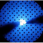
2.1 2 "(50.8mm) Gan HEMT Epitaxial Wafers
We offer 2″(50.8mm) gallium nitride HEMT Wafers, the GaN HEMT structure is as follows:
Struktur (dari atas ke bawah):
* Undoped Gan cap (2 ~ 3nm)
AlxGa1-XN (18 ~ 40nm)
AlN (lapisan penampan)
un-didopkan Gan (2 ~ 3um)
Sapphire substrat
* Kita boleh menggunakan Si3N untuk menggantikan Gan di atas, lekatan yang kuat, ia disalut oleh sputter atau PECVD.
2.2 AlGaN/GaN HEMT Epi Wafer on sapphire/GaN
| Layer # | Kandungan | ketebalan | X | Dopant | Konsentrasi Pembawa |
| 5 | Gan | 2nm | – | – | – |
| 4 | AlxGa1–xN | 8nm | 0.26 | – | – |
| 3 | AlN | 1nm | Un-didopkan | ||
| 2 | Gan | ≥1000 nm | Un-didopkan | ||
| 1 | Lapisan penampan / Peralihan | – | – | ||
| substrat | Silicon | 350μm / 625μm | – | ||
2.3 2″(50.8mm),4″ (100mm)AlGaN/GaN HEMT Epi Wafer on Si
2.3.1 Specifications for Aluminium Gallium Nitride (AlGaN) / Gallium Nitride (Gan) High Electron Mobility Transistor (HEMT) pada substrat silikon.
| keperluan | Spesifikasi |
| AlGaN / Gan HEMT Epi Wafer pada Si | |
| struktur AlGaN / Gan HEMT | rujuk 1.2 |
| substrat bahan | Silicon |
| orientasi | <111> |
| kaedah pertumbuhan | terapung Zon |
| Jenis pengaliran | P atau N |
| Size (inci) | 2 ", 4" |
| Ketebalan (mikron) | 625 |
| Bahagian belakang | kasar |
| Kerintangan (Ω-cm) | >6000 |
| Bow (mikron) | ≤ ± 35 |
2.3.2 Epi structure: Crack-free Epilayers
| Layer # | Kandungan | ketebalan | X | Dopant | Konsentrasi Pembawa |
| 5 | Gan | 2nm | – | – | – |
| 4 | AlxGa1–xN | 8nm | 0.26 | – | – |
| 3 | AlN | 1nm | Un-didopkan | ||
| 2 | Gan | ≥1000 nm | Un-didopkan | ||
| 1 | Lapisan penampan / Peralihan | – | – | ||
| substrat | Silicon | 350μm / 625μm | – | ||
2.3.3 Electrical Properties of the AlGaN/GaN HEMT structure
2DEG Mobility (300 K): ≥1,800 cm2 / Vs
2DEG Lembaran Pembawa Ketumpatan (pada 300 K): ≥0.9 × 1013 cm-2
RMS Kekasaran (AFM): ≤ 0.5 nm (5.0 mikron × 5.0 mikron imbasan Area)
2.4 2″(50.8mm)AlGaN/GaN on sapphire
Untuk spesifikasi AlGaN / Gan pada template nilam, sila hubungi jabatan jualan kami: sales@powerwaywafer.com.
GaN HEMT Applications: Used in blue laser diodes, ultraviolet LEDs (down to 250 nm), and AlGaN/GaN HEMTs device.
3. Explanation of AlGaN/Al/GaN HEMTs:
HEMTs Nitride sedang intensif dibangunkan untuk elektronik berkuasa tinggi dalam frekuensi tinggi penguatan dan pensuisan kuasa aplikasi. Sering prestasi tinggi dalam operasi DC hilang apabila HEMT dihidupkan - sebagai contoh, runtuh dalam semasa apabila isyarat get berdenyut. Ia dikatakan bahawa kesan tersebut adalah berkaitan dengan caj memerangkap bahawa topeng kesan pintu pada aliran semasa. Bidang-pinggan di atas sumber dan pintu elektrod telah digunakan untuk memanipulasi medan elektrik dalam peranti, mengurangkan fenomena semasa runtuh itu.
4. GaN EpitaxialTechnology — Customized GaN epitaxy on SiC,Si and Sapphire substrate for HEMTs, LEDs:
GAN HEMT Epitaxial wafer (GAN EPI-wafer)
PAM XIAMEN Offers Epitaxial growth of AlGaN/GaN based HEMT on Si wafers
5. GaN Device:
Gan HEMT
6. Test Characterization Equipment:
Lembaran sentuh rintangan
Laser Filem Nipis Ketebalan Pemetaan
High Temp / High Kelembapan Reverse Bias
kejutan terma
DIC Nomarski Mikroskop
Atomic Force Microscope (AFM)
Permukaan Defectivity Scan
Temp tinggi Reverse Bias
4PP Lembaran rintangan
Sentuh Dewan Mobility
suhu Cycle
X-ray Diffraction (XRD) / Pantulan (XRR)
Ellipsometer Ketebalan
profilometer
CV Tester
7. Foundry Fabrication:
we also offer foundry GaN HEMT fabrication in the following process as follows:
MOCVD Epitaxy
Metal Sputtering / E-Beam
Kering / Wet Metal / dielektrik Etch
Thin Film PECVD / LPCVD / Sputtering
RTA / Relau Penyepuhlindapan
Photolithography (0.35um min. CD)
ion Implantasi
Remark:
The Chinese government has announced new limits on the exportation of Gallium materials (such as GaAs, GaN, Ga2O3, GaP, InGaAs, and GaSb) and Germanium materials used to make semiconductor chips. Starting from August 1, 2023, exporting these materials is only allowed if we obtains a license from the Chinese Ministry of Commerce. Hope for your understanding and cooperation!
More fabrication services, please visit: GaN Fabrication Services for HEMT Devices
Aluminium gallium arsenide epi wafer
650V GaN FETs Chip for Fast Charge
GaN MOSFET Structure:
GaN MOSFET Structure on SiC Substrate
More about GaN HEMT structures, please read:
Awak juga mungkin menyukai…
-
Gan berasaskan LED Epitaxial Wafer
PAM-XIAMEN’s GaN(gallium nitride)-based LED epitaxial wafer is for ultra high brightness blue and green light emitting diodes (LED) and laser diodes (LD) application.
-
Freestanding Gan substrat
PAM-XIAMEN telah menubuhkan teknologi pembuatan untuk berdiri sendiri (galium nitrida) wafer Gan substrat, yang adalah untuk UHB-LED dan LD. Berkembang dengan teknologi hidrida fasa wap epitaxy (HVPE), substrat Gan kami mempunyai ketumpatan kecacatan rendah.
-
Terapung-Zone Mono-Kristal Silicon
PAM-XIAMEN boleh menawarkan wafer silikon zon terapung, yang diperoleh melalui kaedah Zon Terapung. Rod silikon monohablur diperolehi melalui pertumbuhan zon terapung, dan kemudian memproses rod silikon monohablur menjadi wafer silikon, dipanggil wafer silikon zon terapung. Oleh kerana wafer silikon cair zon tidak bersentuhan dengan pijar kuarza semasa proses silikon zon terapung, bahan silikon berada dalam keadaan terampai. Oleh itu, ia kurang tercemar semasa proses lebur zon terapung silikon. Kandungan karbon dan kandungan oksigen lebih rendah, kekotoran kurang, dan kerintangan lebih tinggi. Ia sesuai untuk pembuatan peranti kuasa dan peranti elektronik voltan tinggi tertentu.
-
Templat Gan
PAM-XIAMEN’s Template Products consist of crystalline layers of (gallium nitride)GaN templates, (aluminum nitride)AlN template,(aluminum gallium nitride) AlGaN templates and (indium gallium nitride) InGaN templates, which are deposited on sapphire -
Ge (Germanium) kristal tunggal dan Wafers
PAM-XIAMEN menawarkan 2”, 3”, 4” dan 6” wafer germanium, yang merupakan singkatan kepada wafer Ge yang ditanam oleh VGF / LEC. Wafer Germanium jenis P dan N yang didop ringan boleh juga digunakan untuk eksperimen kesan Hall. Pada suhu bilik, germanium kristal rapuh dan mempunyai keplastikan yang sedikit. Germanium mempunyai sifat semikonduktor. germanium ketulenan tinggi didopkan dengan unsur trivalen (seperti indium, galium, boron) untuk mendapatkan semikonduktor germanium jenis P; dan unsur pentavalen (seperti antimoni, arsenik, dan fosforus) didopkan untuk mendapatkan semikonduktor germanium jenis N. Germanium mempunyai sifat semikonduktor yang baik, seperti mobiliti elektron tinggi dan mobiliti lubang tinggi. -
Substrat Wafer SiC
Syarikat itu mempunyai barisan pengeluaran substrat wafer SiC(silikon karbida) lengkap yang menyepadukan pertumbuhan kristal, pemprosesan kristal, pemprosesan wafer, penggilap, pembersihan dan ujian. Pada masa kini kami membekalkan wafer SiC 4H dan 6H komersial dengan separa penebat dan kekonduksian dalam paksi atas atau luar paksi, saiz tersedia: 5x5mm2,10x10mm2, 2”,3”,4”, 6” dan 8″, menembusi teknologi utama seperti sebagai penindasan kecacatan, pemprosesan kristal benih dan pertumbuhan pesat, menggalakkan penyelidikan dan pembangunan asas berkaitan epitaksi silikon karbida, peranti, dsb.
-
GaAs Epiwafer
PAM-XIAMEN is manufacturing various types of epi wafer III-V silicon doped n-type semiconductor materials based on Ga, Al, In, As and P grown by MBE or MOCVD. We supply custom GaAs epiwafer structures to meet customer specifications, please contact us for more information.
-
GASB Wafer
PAM-XIAMEN offers Compound Semiconductor GaSb wafer – gallium antimonide which are grown by LEC(Liquid Encapsulated Czochralski) as epi-ready or mechanical grade with n type, p type or semi-insulating in different orientation(111) or (100).


