Kami menawarkan LT-GaAs wafer for THz, detector, ultra-fast-optical experiments and other applications.
1. 2 Spec Spesifikasi Wafer LT-GaAs:
| Perkara | Spesifikasi |
| Diamater (mm) | Ф 50.8mm ± 1mm |
| ketebalan | 1-2um atau 2-3um |
| Marco kecacatan Ketumpatan | ≤ 5 cm-2 |
| Kerintangan (300K) | > 108 Ohm-cm |
| Pembawa | <1ps |
| kehelan Ketumpatan | <1 × 106cm-2 |
| Kawasan permukaan boleh digunakan | ≥80% |
| menggilap | sebelah tunggal digilap |
| substrat | GaAs substrat |
Catatan: Syarat-syarat lain:
1) Substrat GaAs mestilah tidak bertopeng / separa penebat dengan (100) orientasi.
2) Suhu pertumbuhan: ~ 200-250 C
2. Pengenalan LT-GaAs:
GaAs suhu rendah berkembang adalah bahan yang paling banyak digunakan untuk pembuatan pemancar atau pengesan THz fotokonduktif. Ciri uniknya adalah mobiliti pembawa yang baik, ketahanan gelap yang tinggi, dan jangka hayat pembawa subpicosecond.
GaA ditanam oleh epitaxy sinar molekul (MBE) pada suhu lebih rendah daripada 300 ° C (LT GaAs) presents a 1%–2% arsenic excess which depends on the growth temperature Tgand on the arsenic pressure during the deposition. As a result a high density of arsenic antisite defects AsGa is produced and forms a donor miniband close to the center of the band gap. The concentration of AsGa increases with decreasing Tg and can reach 1019–1020 cm-3, which leads to a decrease of the resistivity due to hopping conduction. The concentration of ionized donors AsGa+, which are responsible for the fast electron trapping, depends strongly on the concentration of acceptors (gallium vacancies). The LT-MBE grow GaAs samples are then usually thermally annealed: The excess arsenic precipitates into metallic clusters surrounded by depleted regions of As/GaAs barriers which allow one to recover the high resistivity. The role of the precipitates in the fast carrier recombination process is, however, not yet completely clear. Recently, attempts have been made also to dope LT GaAs during the MBE growth with compensating acceptors, namely with Be, in order to increase the number of AsGa+ : the trapping time reduction was observed for heavily doped samples.
3. Laporan Ujian LT-GaAs:
Sila klik yang berikut untuk melihat laporan LT-GaAs:
https://www.powerwaywafer.com/low-temperature-gaas-2.html
4. Proses Penjanaan THz dalam LT-GaAs
https://www.powerwaywafer.com/THz-Generation-Process-in-LT-GaAs.html
5. Prestasi Antena Fotokonduktif Terahertz:
Sila klik berikut untuk melihat artikel ini:
https://www.powerwaywafer.com/performance-of-terahertz-photoconductive-antennas.html
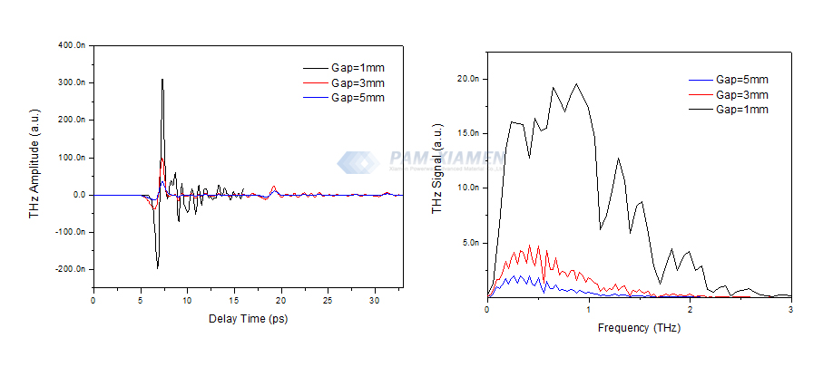
6. Spektrum Domain Masa THz
Di bawah ini adalah Time Domain Spectra THz yang dibuat dari wafer LT-GaAs kami

Spektrum Domain Masa THz
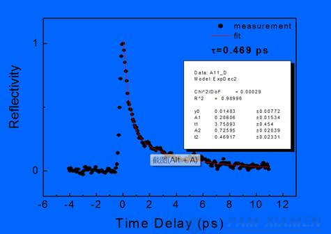
7. Spektrum LT-GaAs Wafer yang diselesaikan secara masa

Spektrum LT-GaAs Wafer yang diselesaikan secara masa
8. FAQ of LT-GaAs Wafer
Q1: Can LT-GaAs substrate be passivated? Does washing the surface with ultrasonics have any effect on that layer of low temperature GaAs?
A: The LT-GaAs substrate can do passivation treatment. It is no problem that wash the surface of LT-GaAs with low-power ultrasonic waves.
Q2: I do photolithography to deposit insulating layer, such as SiO2 100 nm, and metal electrode of Cr 10 nm/ Au 100 nm on LT-GaAs wafer. After the fabrication, I inject a pulsed laser to generate a pulsed charge current. This light-to-charge conversion is done at ambient air at room temperature. The device looks good initially, but after several usage the Au electrode part looks bumpy. (I checked it with a microscope.) I guess the bumpy shape is because water molecules that were unintentionally present in between GaAs and SiO2 or between SiO2 and Cr/Au evaporate by the laser-induced heating. Do have any idea to avoid this issue?
A: We haven’t met this situation before, you can bake the LT GaAs substrate before plating metal, but the temperature should be not too high, below 300 degrees. In addition, you need to rinse the film with dilute acid before making the metal process.
Q3: For low-temperature grown GaAs, we need to work under the scanning tunneling microscope, but the resistivity is too large to tunnel. So, is it possible to reduce the resistivity preferably to below 1M ohm/mm of the epitaxial layer (along the surface direction) by doping? There are no requirements for the elements to be doped and the method of doping.
A: The electrical resistivity of LT-GaAs epi thin film would be able to drop below 1M ohm/mm. Specific technology inquiries please contact victorchan@powerwaywafer.com.
9. Related Products:
GaAs lt wafer
lt-GaAs suis photoconductive
lt-GaAs hidup carrier
lt GaAs THz
batop lt-GaAs
Sumber: PAM-XIAMEN
For more information, please contact us email at victorchan@powerwaywafer.com and powerwaymaterial@gmail.com.

