We specialize in providing antimonide wafers, like InSb wafer: https://www.powerwaywafer.com/compound-semiconductor/insb-wafer.html. In addition, we will offer technology support for you. Here we share a paper “New Process Results in Smoother Indium Antimonide Substrates”, which is about modified chemomechanical polishing of InSb wafer.
Reprinted from: spie.org
Published by:
Patrick Flint, Lisa P. Allen, Gordon Dallas, Daniel Bakken, Kevin Blanchat, Shiva R. Vangala, William Goodhue, David Bliss, and Helen Dauplais
20 August 2009
Modified chemomechanical polishing can reduce five-fold the surface roughness of large-diameter indium antimonide substrates used in advanced imaging systems and devices.
The high optical transparency of indium antimonide (InSb) substrates makes them attractive for IR focal-plane arrays (IRFPAs) and detectors, free-space communications, transistors, and integrated optoelectronics.1–3 A large-diameter crystalline InSb surface can accommodate new and bigger advanced IRFPA designs. However, the 150mm diameter of these antimonides poses unique surface-polishing challenges to substrate manufacturers. To improve the resolution and sensitivity of high-performance IRFPA imaging systems in the 1–5.4μm region (77°K), the substrates’ surface must meet or surpass stringent demands. In particular, for detector-fabrication processes requiring epitaxy growth for the device layer, the starting InSb surface must be ultrasmooth, less than one atomic layer in roughness. It should also desorb the Sb and In surface oxides in an abrupt and fast outgassing process.4 A consistent and easily desorbable surface oxide helps improve advanced-device epilayer yield and performance in Sb-based IRFPA manufacturing.
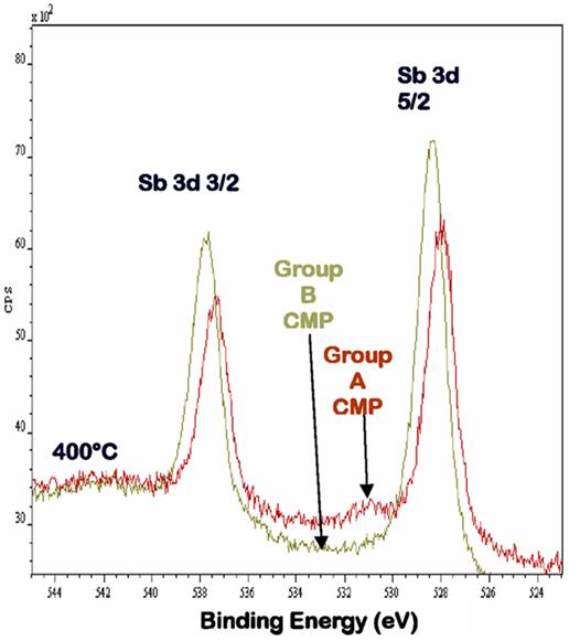
Figure 1. Thermal x-ray photoelectron spectroscopy analysis spectra in electron volts (eV) for the antimonide (Sb) 3d (electron orbital) binding-energy peaks of both Group A and B chemomechanical polish surfaces at 400°C shows the Sb oxide removed for Group B polished surfaces. CMP: Chemomechanical polish.
The substrate’s chemomechanical-polish (CMP) history is a primary factor in InSb surface smoothness and oxide desorption. We wanted to consistently produce surfaces suitable for recent epitaxy processes with stringent substrate-surface specifications. To do so, we analyzed the substrate-surface orientation, atomic roughness, oxide desorption, and crystallinity as a function of CMP process. Our resulting CMP process for larger-diameter InSb single-crystal surfaces has produced a smoother InSb starting surface and abrupt oxide-desorption characteristics suitable for device-layer molecular-beam-epitaxy (MBE) material growth.5
We applied a standard semiconductor-grade CMP to two groups of antimonide substrates separated from the same boule. We used a proprietary CMP process for group A. For group B, we used a process with the same constituents but with a new differential ratio between pH (a measure of the acidity or basicity of a solution) and oxidizer and buffering percentages. Because they were adjacent slices from the same boule, the experiment varied only the polishing constituent ratio. We compared the surfaces by atomic-force microscopy (AFM), Hall-effect doping-concentration analysis, glancing-angle x-ray diffraction (XRD), thermal x-ray photoelectron spectroscopy (TXPS) analysis of surface desorption as a function of temperature, and MBE growth using reflection high-energy electron-diffraction (RHEED) surface-reconstruction patterns.
We found that the group A standard polish retained a distinct presence of residual In and Sb oxides when the InSb surface was heated to 400°C. This is evidenced by the associated oxide peaks of the Sb 3d3/2 (electron orbitals) and In 3d3/2 TXPS spectra as a function of temperature (from room temperature to 450°C). The TXPS data for the group B polish showed that both the Sb 3d3/2 and In 3d3/2 binding-energy peaks completely narrowed, and the associated oxide peaks were absent by 400°C. Figure 1 shows the Sb binding-energy peak comparison. InSb homoepitaxy (MBE and RHEED) results also indicate that group B InSb CMP substrates show an abrupt and desirable 1×1 surface-reconstruction pattern by 430°C in the low-pressure MBE outgassing stage.
Glancing-angle XRD and Hall effect revealed that the crystallinity for group A and B substrates were inherently the same and precisely aligned at InSb(111)B±0.01°. The final epiroughness was significantly higher for group A surfaces than for group B. Typically, as measured by 100μm2 AFM-area images, the epi-atomic roughness (Ra) was 4.7nm, and the peak-to-valley morphology measurements were as high as 84.5nm for the group A surfaces. More significantly, we did not observe any episurface steps or terraces. The surface morphology for group B substrates consisted of clear episteps and terraces with an average Ra of 0.73nm and peak-to-valley heights of 10.7nm.
Various InSb surface-material evaluations of the two CMP processes indicated that group B surfaces allowed a lower temperature and more abrupt surface-oxide-desorption process for epigrowth. The improved low-thermal desorbtion character provided a smooth template for the resulting steps-and-terrace morphology of the InSb episurface.
In summary, the new differential ratio between the pH, the oxidizer percentage, and the buffering percentage of the group B etching solution for InSb surface-oxide removal is effective for InSb(111)B epigrowth surfaces. With a highly desorbable interface, the new InSb CMP finish may provide more widespread adaptation of the crystal for low-power quantum-well-depletion transistors, advanced large-diameter IRFPAs, and optoelectronic applications. We will continue to research improved polishing compounds and processes. We also are working to develop new specifications for larger-diameter substrates.
Author Information
Patrick Flint, operations manager, has more than 17 years of semiconductor engineering experience in manufacturing-improvement programs. He received the 2004 Honeywell Chairman’s Award, the Chairman’s Award Grand Prize, and the 2005 Quest for Excellence Value Creation Award. He graduated with multiple degrees in chemistry and physics from Washington State University (1994), and has numerous publications pertaining to gallium antimonide (GaSb) and indium antimonide (InSb) crystal growth and characterization.
Lisa Allen, technology programs director, has more than 20 years of experience in semiconductor materials research and development. A materials-engineering graduate of the Massachusetts Institute of Technology (MIT) and the University of California at Berkeley, she was the general chair of the 1998 IEEE International Silicon-on-Insulator conference and an executive committee member of the IEEE Nuclear and Space Radiation Effects conference. With more than 120 publications and five patents, she is regional vice president of the MIT Educational Council and a senior member of the IEEE and The Minerals, Metals, & Materials Society.
Gordon Dallas, co-founder, has extensive GaSb and InSb crystal-growth experience. He previously worked at Johnson-Matthey Electronics as a crystal-growth engineer responsible for compound semiconductor crystals for IR detectors. In 1999, he spun off the Johnson-Matthey III–V Substrate unit as Galaxy Compound Semiconductors. Gordon has co-authored numerous antimonide-material conference and journal publications.
Daniel Bakken, co-founder, has received his BS in physics/astrophysics from Eastern Washington University in 1990. He previously worked at Johnson-Matthey Electronics as a crystal-growth engineer responsible for compound semiconductor crystals for IR detectors. In 1999, he spun off the Johnson-Matthey III–V Substrate unit as Galaxy Compound Semiconductors. He has authored numerous antimonide publications.
Shiva R. Vangala, William Goodhue
Photonics Center
University of Massachusetts
Lowell, MA
Shiva Vangala is a postdoctoral research fellow whose research interests include MBE growth and characterization of compound semiconductor structures for optoelectronic and photonic devices such as long-wavelength detectors and quantum-well lasers. He received MS and PhD degrees from the Department of Physics and Applied Physics, University of Massachusetts at Lowell. He is a member of American Physical Society and SPIE.
William Goodhue is a professor in the Department of Physics and a staff member of MIT’s Lincoln Laboratory. His research interests include quantum-well-device physics, photonic and optoelectronic device fabrication, terahertz quantum-cascade lasers, nanosphere lithography applied to quantum-dot technology, and MBE. His work has been reported in numerous articles, reports, book chapters, and meeting speeches. He is a senior member of IEEE.
David Bliss, Helen Dauplais
Sensors Directorate
Air Force Research Laboratory
Hanscom Air Force Base, MA
References:
- P. C. Klipstein, E. Harush, E. Jacobsohn, O. Klin, T. Markovitz, E. Saguy, J. Oiknine-Schlesinger, I. Shtrichman, M. Yassen, E. Weiss, High-performance InAlSb MWIR detectors operating at 100K and beyond, Proc. SPIE6206, pp. 62060M, 2007. doi:10.1117/12.667783
- T. Ashley, A. R. Barnes, L. Buckle, S. Datta, A. B. Dean, Emeny, T. Fearn, D. G. Hayes, K. P. Hilton, R. Jefferies, T. Martin, K. J. Nash, T. J. Phillips, W. H. A. Tang, R. Chau, InSb-based quantum well transistors for high-speed, low-power applications. http://www.gaasmantech.org/Digests/2005/2005papers/14.18.pdf. Accessed 3 August 2009.
- C. J. Hill, A. Soibel, S. A. Keo, J. M. Mumolo, D. Z. Ting, S. D. Gunapala, D. R. Rhiger, R. E. Kvaas, S. F. Harris, Demonstration of mid- and long-wavelength infrared antimonide-based focal plane arrays, Proc. SPIE7298, pp. 729804, 2009. doi:10.1117/12.818692
- O. Klin, S. Grossman, N. Snapi, M. Brumer, I. Lukomsky, M. Yassen, B. Yofis, A. Glozman, A. Zemel, T. Fishman, E. Berkowicz, O. Magen, J. Oiknine-Schlesinger, I. Shtrichman, E. Weiss, P. C. Klipstein, Progress with antimonide-based detectors at SCD, Proc. SPIE7298, pp. 72980G, 2009. doi:10.1117/12.822429
- S. R. Vangala, X. Qian, M. Grzesik, C. Santeufemio, L. P. Allen, G. Dallas, H. Daupliase, K. Vaccaro, S. Q. Wan, D. Bliss, W. D. Goodhue, MBE growth of homoepitaxial layers on CMP processed InSb(100) and InSb(111)B substrates, J. Vac. Sci. Technol. B24, no. 3, pp. 1634-1638, 2006.