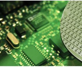


SiC Epitaxy
- Description
Product Description
SiC Epitaxy
PAM-XIAMEN provide custom thin film (silicon carbide) SiC epitaxy on 6H or 4H substrates for the development of silicon carbide devices. SiC epi wafer is mainly used for the fabrication of 600V~3300V power devices, including SBD, JBS, PIN, MOSFET, JFET, BJT, GTO, IGBT, etc. With a silicon carbide wafer as a substrate, a chemical vapor deposition (CVD) method is usually used to deposit a layer of single crystal on the wafer to form an epitaxial wafer. Among them, SiC epitaxy are prepared by growing silicon carbide epitaxial layers on conductive silicon carbide substrates, which can be further fabricated into power devices.
1.Specification of SiC epitaxy:
| Items | Specification | Typical Value |
| Poly-type | 4H | — |
| Off-orientation toward | 4 deg-off | — |
| <11 2_ 0> | ||
| Conductivity | n-type | — |
| Dopant | Nitrogen | — |
| Carrier Concentration | 5E15-2E18 cm-3 | — |
| Tolerance | ± 25% | ± 15% |
| Uniformity | 2”(50.8mm)< 10% | 7% |
| 3”(76.2mm)< 20% | 10% | |
| 4” (100mm)< 20% | 15% | |
| Thickness Range | 5-15 μm | — |
| Tolerance | ± 10% | ± 5% |
| Uniformity | 2”< 5% | 2% |
| 3”< 7% | 3% | |
| 4”< 10% | 5% | |
| Large Point Defects | 2”< 30 | 2”< 15 |
| 3”< 60 | 3”< 30 | |
| 4”< 90 | 4”< 45 | |
| Epi Defects | ≤20 cm-2 | ≤10 cm-2 |
| Step Bunching | ≤2.0nm (Rq) | ≤1.0nm (Rq) |
| (Roughness) |
2 mm edge exclusion for 50.8 and 76.2 mm, 3 mm edge exclusion for 100.0 mmNotes:
• Average of all measurement points for thickness and carrier concentration (see pg. 5)
• N-type epi layers <20 microns are preceeded by n-type, 1E18, 0.5 micron buffer layer
• Not all doping densities are available in all thicknesses
• Uniformity:standard deviation(σ)/average
• Any special requirement on the epi-parameter is on request
2. Introduction of SiC Epitaxy
Why do We Need Silicon Carbide Epitaxial Wafer? Because different from the traditional silicon power device manufacturing process, silicon carbide power devices cannot be directly fabricated on silicon carbide single crystal materials. High-quality epitaxial materials must be grown on conductive single crystal substrates, and various devices manufactured on the SiC epitaxial wafer.
The main epitaxial technology for SiC epitaxy growth is chemical vapor deposition (CVD), which realizes a certain thickness and doped silicon carbide epitaxial material through the growth of SiC epitaxy reactor step flow. With the improvement of silicon carbide power device manufacturing requirements and withstand voltage levels, SiC epi wafer continues to develop in the direction of low defects and thick epitaxy.
In recent years, the quality of thin silicon carbide epitaxial materials (<20 μm) has been continuously improved. The microtubule defects in the epitaxial materials have been eliminated. However, the SiC epitaxy defects, such as drop, triangle, carrot, screw dislocation, basal plane dislocation, deep-level defects, etc., become the main factor affecting device performance. With the advancement of SiC epitaxy process, the thickness of the epitaxial layer has developed from a few μm and tens of μm in the past to the current tens of μm and hundreds of μm. Thanks to the advantages of SiC over Si, the SiC epitaxy market is growing rapidly.
Since silicon carbide devices must be fabricated on epitaxial materials, basically all silicon carbide single crystal materials will be used as SiC epitaxial film to grow epitaxial materials. The technology of silicon carbide epitaxial materials has developed rapidly internationally, with the highest epitaxial thickness reaching more than 250 μm. Among them, the epitaxy technology of 20 μm and below has a high maturity. The surface defect density has been reduced to less than 1/cm2, and the dislocation density has been reduced from 105/cm2 to 103/cm2. The dislocation conversion rate of base plane is close to 100%, which has basically met the requirements of epitaxial materials for large-scale production of silicon carbide devices.
In recent years, the international 30 μm~50 μm epitaxial material technology has also matured rapidly, but due to the limitation of SiC epi market demand, the progress of industrialization has been slow. At present, industrialization company can offer silicon carbide epitaxial materials in batches, include Cree SiC epitaxy, PAM-XIAMEN SiC epitaxy, Dow Corning SiC epitaxy etc..
3.Test Methods
No.1. Carrier concentration:Net doping is determined as an average value across the afer using Hg probe CV.
No.2. Thickness: Thickness is determined as an average value across the wafer using FTIR.
No.3.Large point defects: Microscopic inspection performed at 100X, on an Olympus Optical Microscope, or comparable.
No.4. Epi Defects Inspection or defect map performed under KLA-Tencor Candela CS20 Optical Surface Analyzer or SICA.
No.5. Step bunching: Step bunching and Roughness are scaned by AFM (atomic force microscope) on a 10μm x10μm area
3-1:Large Point Defects Descriptions
Defects which exhibit a clear shape to the unassisted eye and are > 50microns across. These features include spikes, adherent particles, chips andcraters. Large point defects less than 3 mm apart count as one defect.
3-2:Epitaxy Defect Descriptions
SiC epitaxy defects include 3C inclusions, comet tails, carrots, particles, silicon droplets and downfall.
4. Application of SiC epitaxial wafer
Power factor correction(PFC)
PV inverter and UPS(Uninterrupted power supplies) inverters
Motor drives
Output rectification
Hybrid or electric vehicles
SiC Schottky diode with 600V, 650V, 1200V, 1700V, 3300V is available.
Please see below detail application by field:
| Field | Radio Frequency(RF) | Power Device | LED |
| Material | SiLDMOS | Si | GaN/Al2O3 |
| GaAs | GaN/Si | GaN/Si | |
| GaN/SiC | SiC/SiC | GaN/SiC | |
| GaN/Si | Ga203 | / | |
| Device | SiC based GaN HEMT | SiC based MOSFET SiC based BJT SiC based IGBT SiC based SBD |
/ |
| Application | Radar, 5G | Electric vehicles | Solid State Lighting |
5. Mechanical wafers with Epi layes: are available, such as for process monitoring, which require wafers with low bow and warpage.
150mm 4H n-type SiC EPI wafers
Intrinsic SiC Epilayer on Silicon carbide substrate
Why do We Need Silicon Carbide Epitaxial Wafer?
SiC MOSFET Structure Homoepitaxial on SiC substrate
You may also like…
-
SIC Application
Due to SiC physical and electronic properties,Silicon Carbide based device are well suitable for short wavelength optoelectronic, high temperature, radiation resistant, and high-power/high-frequency electronic devices,compared with Si and GaAs device -
SiC Wafer Substrate
The company has a complete SiC(silicon carbide) wafer substrate production line integrating crystal growth, crystal processing, wafer processing, polishing, cleaning and testing. Nowadays we supply commercial 4H and 6H SiC wafers with semi insulation and conductivity in on-axis or off-axis, available size:5x5mm2,10x10mm2, 2”,3”,4”, 6” and 8″, breaking through key technologies such as defect suppression, seed crystal processing and rapid growth, promoting basic research and development related to silicon carbide epitaxy, devices, etc.
-
Cz Mono-Crystalline Silicon
PAM-XIAMEN, a monocrystalline bulk silicon producer, can offer <100>, <110> and <111> monocrystalline silicon wafers with N&P dopant in 76.2~200 mm, which are grown by CZ method. The Czochralski method is a crystal growth method, referred to as the CZ method. It is integrated in a straight-tube heat system, heated by graphite resistance, melts the polysilicon contained in a high-purity quartz crucible, and then inserts the seed crystal into the surface of the melt for welding. After that, the rotating seed crystal is lowered and melted. The body is infiltrated and touched, gradually raised, and finished or pulled through the steps of necking, necking, shouldering, equal diameter control, and finishing.
-
InP wafer
PAM-XIAMEN offers VGF InP(Indium Phosphide) wafer with prime or test grade including low dope, N type or semi-insulating. The mobility of InP wafer is different in different type, low doped one>=3000cm2/V.s, N type>1000 or 2000cm2V.s(depends on different doping concentration), P type: 60+/-10 or 80+/-10cm2/V.s(depends on different Zn doping concentration), and semi-insulting one>2000cm2/V.s, the EPD of Indium Phosphide is below 500/cm2 normally.
-
SiC Wafer Reclaim
PAM-XIAMEN is able to offer the following SiC reclaim wafer services.
-
GaAs Epiwafer
PAM-XIAMEN is manufacturing various types of epi wafer III-V silicon doped n-type semiconductor materials based on Ga, Al, In, As and P grown by MBE or MOCVD. We supply custom GaAs epiwafer structures to meet customer specifications, please contact us for more information.
-
Freestanding GaN substrate
PAM-XIAMEN has established the manufacturing technology for freestanding (gallium nitride)GaN substrate wafer, which is for UHB-LED and LD. Grown by hydride vapour phase epitaxy (HVPE) technology,Our GaN substrate has low defect density.
-
Ge(Germanium) Single Crystals and Wafers
PAM-XIAMEN offers 2”, 3”, 4” and 6” germanium wafer, which is short for Ge wafer grown by VGF / LEC. Lightly doped P and N type Germanium wafer can be also used for Hall effect experiment. At room temperature, crystalline germanium is brittle and has little plasticity. Germanium has semiconductor properties. High-purity germanium is doped with trivalent elements (such as indium, gallium, boron) to obtain P-type germanium semiconductors; and pentavalent elements (such as antimony, arsenic, and phosphorus) are doped to obtain N-type germanium semiconductors. Germanium has good semiconductor properties, such as high electron mobility and high hole mobility.