PAM-XIAMEN offers SiC-on-SiC epi wafer for pin-diodes (p-n junction SiC epi wafer) as follows:
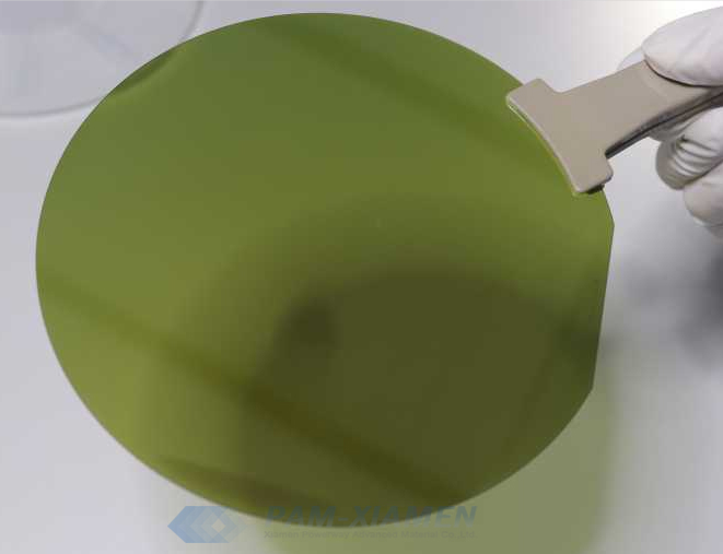
SiC-On-SiC Epi Wafer For Pin-Diodes
1. Specifications of SiC Epitaxy on Silicon Carbide Substrate
pin-diodes structure 1: SiC-on-SiC epi-wafer PAM060320-SIC
p+[Al]: 5 µm, gradient doping, Na-Nd = 5*10^18 – 1*10^20 ± 50% cm-3
p[Al]: 20 µm, Na-Nd = 4.9*10^15 cm-3
n+[N]: 2 µm, Na-Nd = 5*10^18 ± 25% cm-3
substrate: 4H, ∅ 4″ (100 mm), h = 350 µm, ρv = 0.012-0.0025 Ohm*cm; 4° off to <11-20>; MPD: 0 (high purity) cm-2
pin-diodes structure 2: SiC-on-SiC epi-wafer PAM060420-SIC
p+[Al]: 5 µm, gradient doping, Na-Nd = 5*10^18 – 1*10^20 ± 50% cm-3
p[Al]: 20 µm, Na-Nd = 4.9*10^15 cm-3
n+[N]: 2 µm, Na-Nd = 5*10^18 ± 25% cm-3
substrate: 4H, ∅ 4″ (100 mm), h = 350 µm, ρv = 0.012-0.0025 Ohm*cm; 4° off to <11-20>; MPD: <=5 cm-2
pin-diodes structure 3: 4H SiC P-I-N Structure PAM201214-PIN
4-in SIC epiwafers
Diameter:100mm,
Thickness:350um thick;
n-type 4H-SiC,
4-degree off-axis,
Buffer Thickness: 0.5um,n-type, Doping level:1E18cm-3
Epi:Thickness: 30um+/-5%, n-Doping level:<=1E14cm-3
*Surface defect density≤0.8/cm2;
*Surface roughnesss 2nm;
*Scratches cumulative(max5) less than 1dia.
2. About SiC PIN Diodes
SiC pin diodes have a switching speed of 2 to 3 orders of magnitude higher than that of Si, high junction temperature tolerance, high current density, and higher power density.
① The breakdown electric field is increased by nearly an order of magnitude: thinner and higher doping concentration barrier layers can be used in the design;
②Three times the height of the wide band gap: makes it have a higher working temperature and higher radiation resistance; but this also makes its built-in electric potential three times higher than that of Si;
③The thermal conductivity(4.9K/W) is three times higher than that of Si: it makes the heat dissipation performance higher and can achieve higher power.
SiC pin diode has a very small reverse recovery charge QRR compared with Si-based diodes at the same level. The main reasons are as follows:
The voltage blocking layer is thinned by tens of times, and the doping concentration is higher than several tens of times, which makes the minority carrier charge in the intrinsic layer significantly reduced;
The carrier life required for these thinner voltage barriers is shorter than that of Si at more than 10 times; and the SiC pin diodes fabricated on p-n junction wafers have a very high temperature forward voltage drop when the temperature changes.
3. Industrial Norms of SiC Single Crystal Epitaxial Wafer on SiC Thin Film
3.1 SiC Substrate Parameters for SiC Epitaxy Growth
The doping concentration of the single crystal silicon carbide substrate should meet the requirements of Table 1:
Table 1
| Conductivity Type | Dopant | Plane | SiC Single Crystal Diameter/mm | Concentration/(cm3) |
| N | N | C plane | 76.2、100、150 | 1E16~~1E19 |
| Si plane | 76.2、100、150 | 9E14~1E19 | ||
| P | Al | Si plane | 76.2、100、150 | 9E14~1E19 |
3.2 SiC Epitaxial Wafer Doping Concentration
The doping element of the N-type SiC epitaxial layer on silicon carbide wafer is nitrogen, and the doping element of the P-type epitaxial layer of silicon carbide on SiC wafer is aluminum.
In addition, during silicon carbide epitaxial growth, the average concentration of the SiC epitaxial film layer and its allowable deviation should be controlled as stipulated in Table 2:
Table 2
| Average Concentration/cm3 | Allowable Deviation/% | |
| N type | P type | |
| 9E14~1E19 | ±25 | ±50 |
The radial concentration variation of the silicon carbide epitaxial layer on SiC substrate should meet the requirements of Table 3.
Table 3
| Average Concentration/cm3 | Radial Concentration Variation/% | |
| N type | P type | |
| 9E14~1E19 | ≤15 | ≤20 |
3.3 Epitaxial Layer Thickness on the Silicon Carbide Substrate
The thickness of the SiC epilayer, the allowable deviation and the radial thickness variation of the SiC epi layer shall meet the requirements of Table 4.
Table 4
| Average Thickness/ u m | Allowable Deviation/% | Radial Thickness Variation/% |
| 0.2~50 | ±10 | ≤10 |
3.4 Defects of SiC-on-SiC Epi Wafer
The limit of defects shall meet the requirements of Table 5.
Table 5
| No. | Defects | Limit | |
| 1 | Point defect | ≤5/cm2 | |
| 2 | Chipping | Within 1.5mm radius, the quantity does not exceed 2 | |
| 3 | Scratches | The number does not exceed 10, and the total length does not exceed 1 diameter | |
| 4 | Giant steps | 4° | Not applicable |
| 8° | Area ≤5% | ||
| 5 | Clean area on the back | ≥95% | |
The surface defect area refers to: for the silicon carbide epitaxial wafer with a diameter of 76.2mm, the entire surface of the 2mm ring area is removed from the edge, and the entire surface of the 100mm & 150mm silicon carbide epitaxial wafer is removed from the edge 3mm ring area;
Point defects include triangular defects, drips and carrots;
Edge chipping refers to the defect that the edge of the epitaxial wafer is accidentally peeled of;
Scratches are non-removable linear traces with an aspect ratio of more than 5 left on the surface of the SiC epitaxial wafer due to scratches by foreign objects;
A giant step is a visible parallel linear defect perpendicular to the main reference edge;
If the customer has special demands for N type or P type single crystal SiC-on-SiC epi wafer, it shall be negotiated by both parties.
4. FAQ of SiC on SiC
Q: How can you guarantee (show evidence) that the carrier concentration of p-SiC on SiC is ≤5E14? I believe that ECV method, which are commonly used to measure carrier concentration, are not capable of measuring carrier concentration this low. What kind of method are you using?
A: We can use *** method to test the carrier concentration of SiC epitaxy after you order. Please contact victorchan@powerwaywafer.com for *** value.

For more information, please contact us email at victorchan@powerwaywafer.com and powerwaymaterial@gmail.com