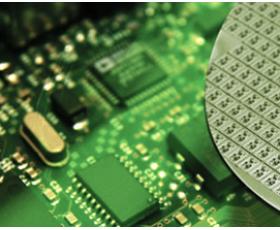


SiC Epitaxy
- Penerangan
Penerangan Produk
SiC Epitaxy
PAM-XIAMEN menyediakan filem nipis tersuai (silikon karbida) epitaksi SiC pada substrat 6H atau 4H untuk pembangunan peranti silikon karbida. Wafer epi SiC digunakan terutamanya untuk fabrikasi peranti kuasa 600V~3300V, termasuk SBD, JBS, PIN, MOSFET, JFET, BJT, GTO, IGBT, dll. Dengan wafer silikon karbida sebagai substrat, pemendapan wap kimia (CVD ) kaedah biasanya digunakan untuk mendepositkan lapisan kristal tunggal pada wafer untuk membentuk wafer epitaxial. Antaranya, epitaksi SiC disediakan dengan menumbuhkan lapisan epitaxial silikon karbida pada substrat silikon karbida konduktif, yang boleh dibuat lagi menjadi peranti kuasa.
1. Spesifikasi epitaxy SiC:
| barangan | Spesifikasi | Nilai tipikal |
| Poly-jenis | 4H | — |
| Off-orientasi ke arah | 4 deg-off | — |
| <11 2_ 0> | ||
| kekonduksian | n-jenis | — |
| Dopant | Nitrogen | — |
| Konsentrasi Pembawa | 5E15-2E18 cm-3 | — |
| toleransi | ± 25% | ± 15% |
| keseragaman | 2 "(50.8mm) <10% | 7% |
| 3 "(76.2 mm) <20% | 10% | |
| 4 "(100mm) <20% | 15% | |
| Julat ketebalan | 5-15 mikron | — |
| toleransi | ± 10% | ± 5% |
| keseragaman | 2 "<5% | 2% |
| 3 "<7% | 3% | |
| 4 "<10% | 5% | |
| Kecacatan Point besar | 2 "<30 | 2 "<15 |
| 3 "<60 | 3 "<30 | |
| 4 "<90 | 4 "<45 | |
| Kecacatan Epi | ≤20 cm-2 | ≤10 cm-2 |
| bunching langkah | ≤2.0nm (Rq) | ≤1.0nm (Rq) |
| (Kekasaran) |
Pengecualian tepi 2 mm untuk 50.8 dan 76.2 mm, pengecualian tepi 3 mm untuk 100.0 mm Catatan:
• Purata semua titik pengukuran untuk ketebalan dan kepekatan pembawa (lihat halaman 5)
• Lapisan epi jenis N <20 mikron didahului oleh lapisan penyangga n-type, 1E18, 0.5 mikron
• Tidak semua ketumpatan doping tersedia dalam semua ketebalan
• Keseragaman: sisihan piawai (σ) / purata
• Keperluan khas pada parameter epi adalah berdasarkan permintaan
2. Pengenalan SiC Epitaxy
Mengapa Kami Memerlukan Wafer Epitaxial Silicon Carbide?Kerana berbeza daripada proses pembuatan peranti kuasa silikon tradisional, peranti kuasa silikon karbida tidak boleh dibuat secara langsung pada bahan kristal tunggal silikon karbida. Bahan epitaxial berkualiti tinggi mesti ditanam pada substrat kristal tunggal konduktif, dan pelbagai peranti yang dihasilkan pada wafer epitaxial SiC.
Teknologi epitaksi utama untuk pertumbuhan epitaksi SiC ialah pemendapan wap kimia (CVD), yang merealisasikan ketebalan tertentu dan bahan epitaksi silikon karbida terdop melalui pertumbuhan aliran langkah reaktor epitaksi SiC. Dengan peningkatan keperluan pembuatan peranti kuasa silikon karbida dan menahan tahap voltan, wafer epi SiC terus berkembang ke arah kecacatan rendah dan epitaksi tebal.
Dalam beberapa tahun kebelakangan ini, kualiti bahan epitaxial silikon karbida nipis (<20 μm) telah dipertingkatkan secara berterusan. Kecacatan mikrotubul dalam bahan epitaxial telah dihapuskan. Walau bagaimanapun, kecacatan epitaksi SiC, seperti kejatuhan, segi tiga, lobak merah, kehelan skru, kehelan satah basal, kecacatan tahap dalam, dll., menjadi faktor utama yang mempengaruhi prestasi peranti. Dengan kemajuan proses epitaksi SiC, ketebalan lapisan epitaxial telah berkembang daripada beberapa μm dan puluhan μm pada masa lalu kepada puluhan μm dan ratusan μm semasa. Terima kasih kepada kelebihan SiC berbanding Si, pasaran epitaksi SiC berkembang pesat.
Oleh kerana peranti silikon karbida mesti dibuat pada bahan epitaxial, pada asasnya semua bahan kristal tunggal silikon karbida akan digunakan sebagai filem epitaxial SiC untuk mengembangkan bahan epitaxial. Teknologi bahan epitaxial silikon karbida telah berkembang pesat di peringkat antarabangsa, dengan ketebalan epitaxial tertinggi mencapai lebih daripada 250 μm. Antaranya, teknologi epitaksi 20 μm ke bawah mempunyai kematangan yang tinggi. Ketumpatan kecacatan permukaan telah dikurangkan kepada kurang daripada 1/cm2, dan ketumpatan kehelan telah dikurangkan daripada 105/cm2 kepada 103/cm2. Kadar penukaran kehelan satah asas adalah hampir 100%, yang pada asasnya telah memenuhi keperluan bahan epitaxial untuk pengeluaran peranti silikon karbida secara besar-besaran.
Dalam tahun-tahun kebelakangan ini, teknologi bahan epitaxial antarabangsa 30 μm~50 μm juga telah matang dengan cepat, tetapi disebabkan oleh pengehadan permintaan pasaran epi SiC, kemajuan perindustrian menjadi perlahan. Pada masa ini, syarikat perindustrian boleh menawarkan bahan epitaxial silikon karbida dalam kelompok, termasuk epitaksi Cree SiC, epitaksi PAM-XIAMEN SiC, epitaksi Dow Corning SiC dll.
3. Kaedah Ujian
No.1. kepekatan pembawa: doping Net ini telah dipilih sebagai nilai purata seluruh afer menggunakan Hg siasatan CV.
No.2. Ketebalan: Ketebalan ini telah dipilih sebagai nilai purata seluruh wafer menggunakan FTIR.
kecacatan titik No.3.Large: pemeriksaan mikroskopik dilakukan pada 100X, atas optik mikroskop Olympus, atau setanding.
No.4. Pemeriksaan Kecacatan Epi atau peta kecacatan yang dilakukan di bawah KLA-Tencor Candela CS20 Optical Surface Analyzer atau SICA.
No.5. Langkah bunching: Langkah bunching dan Kekasaran sedang scaned oleh AFM (daya atom mikroskop) di kawasan x10μm 10μm
3-1:Perihalan Kecacatan Mata Besar
Kecacatan yang mempamerkan bentuk yang jelas dengan mata tanpa bantuan dan> 50microns seluruh. Ciri-ciri ini termasuk pancang, zarah pengikut, cip andcraters. kecacatan titik besar kurang daripada 3 mm selain dikira sebagai satu kecacatan.
3-2: Penerangan Kecacatan Epitaksi
Kecacatan epitaksi SiC termasuk kemasukan 3C, ekor komet, lobak merah, zarah, titisan silikon dan kejatuhan.
4. Penggunaan wafer epitaxial SiC
pembetulan faktor kuasa (PFC)
PV penyongsang dan (bekalan kuasa tanpa gangguan) penyongsang UPS
pemacu motor
pembetulan output
Hibrid atau elektrik kenderaan
SiC Schottky Diod dengan 600V, 650V, 1200V, 1700V, 3300V boleh didapati.
Sila lihat aplikasi terperinci di bawah mengikut bidang:
| Padang | Frekuensi Radio (RF) | Peranti Kuasa | LED |
| Bahan | SiLDMOS | Si | GaN / Al2O3 |
| GaAs | GaN / Si | GaN / Si | |
| GaN / SiC | SiC / SiC | GaN / SiC | |
| GaN / Si | Ga203 | / | |
| Peranti | GaN HEMT berasaskan SiC | MOSFET berasaskan SiC BJT berasaskan SiC IGBT berasaskan SiC SBD berasaskan SiC |
/ |
| Permohonan | Radar, 5G | Kenderaan elektrik | Pencahayaan Keadaan Pepejal |
5. Wafer mekanikal dengan lapisan Epi: tersedia, seperti untuk pemantauan proses, yang memerlukan wafer dengan busur rendah dan melengkung.
150mm 4H n-jenis wafer SiC EPI
Epilayer SiC Intrinsik pada substrat Silicon karbida
Mengapa Kami Memerlukan Wafer Epitaxial Silicon Carbide?
Struktur MOSFET SiC Homoepitaxial pada substrat SiC
Awak juga mungkin menyukai…
-
SiC Wafer Substrat
The company has a complete SiC(silicon carbide) wafer substrate production line integrating crystal growth, crystal processing, wafer processing, polishing, cleaning and testing. Nowadays we supply commercial 4H and 6H SiC wafers with semi insulation and conductivity in on-axis or off-axis, available size:5x5mm2,10x10mm2, 2”,3”,4”, 6” and 8″, breaking through key technologies such as defect suppression, seed crystal processing and rapid growth, promoting basic research and development related to silicon carbide epitaxy, devices, etc.
-
Ge (Germanium) kristal tunggal dan Wafers
PAM-XIAMEN menawarkan wafer germanium 2", 3", 4" dan 6", yang merupakan singkatan untuk wafer Ge yang ditanam oleh VGF / LEC. Wafer Germanium jenis P dan N yang didop ringan boleh juga digunakan untuk eksperimen kesan Hall. Pada suhu bilik, germanium kristal rapuh dan mempunyai keplastikan yang sedikit. Germanium mempunyai sifat semikonduktor. germanium ketulenan tinggi didopkan dengan unsur trivalen (seperti indium, galium, boron) untuk mendapatkan semikonduktor germanium jenis P; dan unsur pentavalen (seperti antimoni, arsenik, dan fosforus) didopkan untuk mendapatkan semikonduktor germanium jenis N. Germanium mempunyai sifat semikonduktor yang baik, seperti mobiliti elektron tinggi dan mobiliti lubang tinggi. -
SIC Permohonan
Oleh kerana SiC sifat fizikal dan elektronik, peranti Silicon Carbide berdasarkan dengan baik sesuai untuk optoelektronik pendek panjang gelombang, suhu tinggi, tahan radiasi, dan berkuasa tinggi / frekuensi tinggi peranti elektronik, berbanding dengan Si dan GaAs peranti -
Freestanding Gan substrat
PAM-XIAMEN telah menubuhkan teknologi pembuatan untuk berdiri sendiri (galium nitrida) wafer Gan substrat, yang adalah untuk UHB-LED dan LD. Berkembang dengan teknologi hidrida fasa wap epitaxy (HVPE), substrat Gan kami mempunyai ketumpatan kecacatan rendah.
-
Cz Mono-Kristal Silicon
PAM-XIAMEN, pengeluar silikon pukal monohablur, boleh menawarkan wafer silikon monohablur <100>, <110> dan <111> dengan dopan N&P dalam 76.2~200 mm, yang ditanam dengan kaedah CZ. Kaedah Czochralski ialah kaedah pertumbuhan kristal, dirujuk sebagai kaedah CZ. Ia disepadukan dalam sistem haba tiub lurus, dipanaskan oleh rintangan grafit, mencairkan polysilicon yang terkandung dalam mangkuk kuarza ketulenan tinggi, dan kemudian memasukkan kristal benih ke dalam permukaan cair untuk kimpalan. Selepas itu, kristal benih yang berputar diturunkan dan cair. Badan disusup dan disentuh, secara beransur-ansur dinaikkan, dan selesai atau ditarik melalui langkah-langkah menekuk, menekuk, memikul, kawalan diameter yang sama, dan kemasan.
-
SiC Wafer Reclaim
PAM-XIAMEN mampu menawarkan yang SiC berikut menuntut semula perkhidmatan wafer.
-
wafer InP
PAM-XIAMEN offers VGF InP(Indium Phosphide) wafer with prime or test grade including low dope, N type or semi-insulating. The mobility of InP wafer is different in different type, low doped one>=3000cm2/V.s, N type>1000 or 2000cm2V.s(depends on different doping concentration), P type: 60+/-10 or 80+/-10cm2/V.s(depends on different Zn doping concentration), and semi-insulting one>2000cm2/V.s, the EPD of Indium Phosphide is below 500/cm2 normally.
-
GaAs Epiwafer
PAM-XIAMEN mengeluarkan pelbagai jenis bahan semikonduktor jenis-n doped epi wafer III-V silikon berasaskan Ga, Al, In, As dan P yang ditanam oleh MBE atau MOCVD. Kami membekalkan struktur epiwafer GaAs tersuai untuk memenuhi spesifikasi pelanggan, sila hubungi kami untuk mendapatkan maklumat lanjut.