
Silikon Mono-Kristal Zon Float
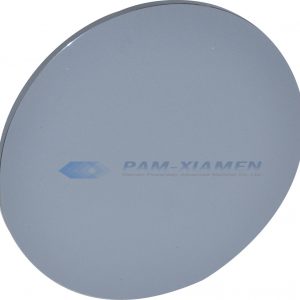
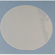
PAM-XIAMEN can offer float zone silicon wafer, which is obtained by Float Zone method. Monocrystalline silicon rods is got through float zone growth, and then process the monocrystalline silicon rods into silicon wafers, called float zone silicon wafers. Since the zone-melted silicon wafer is not in contact with the quartz crucible during the floating zone silicon process, the silicon material is in a suspended state. Thereby, it is less polluted during the process of floating zone melting of silicon. The carbon content and oxygen content are lower, the impurities are less, and the resistivity is higher. It is suitable for the manufacture of power devices and certain high-voltage electronic devices.
- Penerangan
Penerangan Produk
PAM-XIAMEN can offer float zone silicon wafer, which is obtained by Float Zone method. Monocrystalline silicon rods is got through float zone growth, and then process the monocrystalline silicon rods into silicon wafers, called float zone silicon wafers. Since the zone-melted silicon wafer is not in contact with the quartz crucible during the floating zone silicon process, the silicon material is in a suspended state. Thereby, it is less polluted during the process of floating zone melting of silicon. The carbon content and oxygen content are lower, the impurities are less, and the resistivity is higher. It is suitable for the manufacture of power devices and certain high-voltage electronic devices.
1. Float zone silicon wafer specification
| ype | Jenis pengaliran | orientasi | Diameter (mm) | Kekonduksian (Ω • cm) |
| Rintangan tinggi | N & P | <100> & <111> | 76.2-200 | >1000 |
| NTD | N | <100> & <111> | 76.2-200 | 30-800 |
| CFZ | N & P | <100> & <111> | 76.2-200 | 1-50 |
| GD | N & P | <100> & <111> | 76.2-200 | 0.001-300 |
1.1 Floating zone silicon wafer specification
| Parameter Ingot | Item | Penerangan |
| Kaedah berkembang | FZ | |
| orientasi | <111> | |
| Off-orientasi | 4 ± 0.5 darjah ke <110> yang terdekat | |
| Jenis / Dopant | P / Boron | |
| kerintangan | 10-20 W.cm | |
| RRV | ≤15% (Max edge-Cen) / Sen |
1.2 FZ silicon wafer specification
| meter | Item | Penerangan |
| diameter | 150 ± 0.5 mm | |
| ketebalan | 675 ± 15 um | |
| Negara Flat utama | 57.5 ± 2.5 mm | |
| Orientation Flat utama | <011> ± 1 darjah | |
| Menengah Flat Negara | Tiada | |
| Orientation Flat menengah | Tiada | |
| TTV | ≤5 um | |
| Bow | ≤40 um | |
| Warp | ≤40 um | |
| Profil Tepi | Piawaian SEMI | |
| Permukaan Depan | Penggilap Mekanikal Kimia | |
| LPD | ≥0.3 um @ ≤15 pcs | |
| Permukaan Belakang | Asid Terukir | |
| Cip Tepi | Tiada | |
| Pakej | Pembungkusan Vakum; Plastik Dalaman, Aluminium Luar |
2. Float-zone mono-crystalline silicon classifications
2.1 FZ-Silicon
The mono-crystalline silicon with the characteristics of low foreign-material content, low defect density and perfect crystal structure is produced with the float zone silicon process; no foreign material is introduced during the float zone silicon crystal growth. The FZ-Silicon conductivity is usually above 1000 Ω-cm, and such a high resistivity float zone silicon is mainly used to produce the high inverse-voltage elements and photoelectronic devices. It also can be used for dry etching process.
2.2 NTDFZ-Silicon
The mono-crystalline silicon with high-resistivity and uniformity can be achieved by neutron irradiation of FZ-silicon, to ensure the yield and uniformity of produced elements, and is mainly used to produce the silicon rectifier (SR), silicon control (SCR), giant transistor (GTR), gate-turn-off thyristor (GTO), static induction thyristor (SITH), insulate-gate bipolar transistor (IGBT), extra HV diode (PIN), smart power and power IC, etc; it is the main functional material for various frequency converters, rectifiers, large-power control elements, new power electronic devices, detectors, sensors, photoelectronic devices and special power devices.
FZ NTD Silicon Wafer with a Uniform Doping Concentration
2.3 GDFZ-Silicon
Utilizing the foreign-material diffusion mechanism, add the gas-phase foreign-material during the floating zone monocrystalline silicon process, to solve the doping problem of float-zone process from the root, and to get the GDFZ-silicon which is N-type or P-type, has the resistivity 0.001-300 Ω.cm, relative good resistivity uniformity and neutron irradiation. It is applicable for producing various semi-conductor power elements, insulate-gate bipolar transistor (IGBT) and high-efficiency solar cell, etc.
2.4 CFZ-Silicon
Silikon monokristalin dihasilkan dengan kombinasi proses Czochralski dan zon apungan, dan mempunyai kualiti antara silikon monokristalin CZ dan silikon monokristalin FZ; elemen khas boleh didoping, seperti Ga, Ge dan lain-lain. Wafer solar silikon CFZ generasi baru lebih baik daripada pelbagai wafer silikon dalam industri PV global pada setiap indeks prestasi; kecekapan penukaran panel solar adalah hingga 24-26%. Produk ini terutama digunakan dalam bateri solar dengan kecekapan tinggi dengan struktur khas, kontak belakang, HIT dan proses khas lain, dan lebih banyak digunakan dalam LED, elemen kuasa, automobil, satelit dan pelbagai produk dan bidang lain.
Kelebihan kami sepintas lalu
peralatan pertumbuhan epitaxy 1. lanjutan dan peralatan ujian.
2.Offer the highest quality with low defect density and good float zone silicon surface roughness.
3. kuat sokongan pasukan penyelidikan dan sokongan teknologi untuk pelanggan-pelanggan kami
Si MEMS Wafer Grown by FZ
4 ″ FZ Prime Silicon Wafer
3 "FZ Perdana Silicon Wafer Ketebalan: 350 ± 15um
4 Th Ketebalan FZ Prime Silicon Wafer: 400µm +/- 25µm
4 Th Ketebalan FZ Prime Silicon Wafer: 400µm +/- 25µm-2
4 ″ FZ Silicon Ingot dengan Diameter 100.7 ± 0.3mm
3 "FZ Silicon Wafer Ketebalan: 229-249μm -1
3 "FZ Silicon Wafer Ketebalan: 229-249μm -2
FZ Intrinsic wafer Silicon undoped
1 ″ FZ Silicon Ingot dengan Diameter 25mm
2 ″ FZ Silicon Ingot dengan Diameter 50mm
4″ FZ Intrinsic Silicon Wafer SSP
4″ FZ Intrinsic Silicon Wafer DSP
3 ″ FZ Silicon Ingot dengan Diameter 76mm
6 ″ FZ Silicon Wafer dengan Diameter 150mm, Kedua-dua Bahagian Terukir
Awak juga mungkin menyukai…
-
SiC Wafer Substrat
The company has a complete SiC(silicon carbide) wafer substrate production line integrating crystal growth, crystal processing, wafer processing, polishing, cleaning and testing. Nowadays we supply commercial 4H and 6H SiC wafers with semi insulation and conductivity in on-axis or off-axis, available size:5x5mm2,10x10mm2, 2”,3”,4”, 6” and 8″, breaking through key technologies such as defect suppression, seed crystal processing and rapid growth, promoting basic research and development related to silicon carbide epitaxy, devices, etc.
-
Cz Mono-Kristal Silicon
PAM-XIAMEN, a monocrystalline bulk silicon producer, can offer <100>, <110> and <111> monocrystalline silicon wafers with N&P dopant in 76.2~200 mm, which are grown by CZ method. The Czochralski method is a crystal growth method, referred to as the CZ method. It is integrated in a straight-tube heat system, heated by graphite resistance, melts the polysilicon contained in a high-purity quartz crucible, and then inserts the seed crystal into the surface of the melt for welding. After that, the rotating seed crystal is lowered and melted. The body is infiltrated and touched, gradually raised, and finished or pulled through the steps of necking, necking, shouldering, equal diameter control, and finishing.
-
Epitaxial Silicon Wafer
Silicon Epitaxial Wafer(Epi Wafer) is a layer of epitaxial silicon single crystal deposited onto a single crystal silicon wafer(note: it is available to grow a layer of poly crystalline Silicon layer on top of a highly doped Singly crystalline silicon wafer, but it needs buffer layer (such as oxide or poly-Si) in between the bulk Si substrate and the top epitaxial silicon layer. It also can be used for thin film transistor.
-
GaAs Epiwafer
PAM-XIAMEN is manufacturing various types of epi wafer III-V silicon doped n-type semiconductor materials based on Ga, Al, In, As and P grown by MBE or MOCVD. We supply custom GaAs epiwafer structures to meet customer specifications, please contact us for more information.
-
Wafer digilap
PAM-XIAMEN can offer polished wafer, n type or p type with orientation at <100>, <110> or <111>. FZ polished wafers, mainly for the production of silicon rectifier (SR), silicon controlled rectifier (SCR), Giant Transistor (GTR), thyristor (GRO)
-
punaran Wafer
The etching silicon wafers offered by PAM-XIAMEN are N type or P type etching wafers, which have low roughness, low reflectivity and high reflectivity. The etching wafer has the characteristics of low roughness, good glossiness and relatively low cost, and directly substitutes the polished wafer or epitaxial wafer which has relatively high cost to produce the electronic elements in some fields, reducing the costs.
-
Ujian Wafer Monitor Wafer Dummy Wafer
As a dummy wafer manufacturer, PAM-XIAMEN offers silicone dummy wafer / test wafer / monitor wafer, which is used in a production device to improve safety in the beginning of production process and are used for delivery check and evaluation of process form. As dummy silicon wafers are often used for experiment and test, size and thickness thereof are important factors in most occasions. 100mm, 150mm, 200mm, or 300mm dummy wafer is available.
-
Freestanding Gan substrat
PAM-XIAMEN telah menubuhkan teknologi pembuatan untuk berdiri sendiri (galium nitrida) wafer Gan substrat, yang adalah untuk UHB-LED dan LD. Berkembang dengan teknologi hidrida fasa wap epitaxy (HVPE), substrat Gan kami mempunyai ketumpatan kecacatan rendah.


Produk Berkaitan
-
12 "Silicon wafer 300mm TOX (Si Thermal Oxidation Wafer)
PAM-XIAMEN offers 300mm silicon oxide wafer and dioxide wafer. Thermal oxide silicon wafer or silicon dioxide wafer is a bare silicon wafer with oxide layer grown by dry or wet oxidation process. The thermal oxide layer of the silicon wafer is usually grown in a horizontal tube furnace, and the silicon wafer oxide temperature range is generally 900 ℃ ~ 1200 ℃. Compared with CVD oxide layer, silicon wafer oxide layer has higher uniformity, better compactness, higher dielectric strength and better quality.
-
12 "Perdana Gred Silicon Wafer
PAM-XIAMEN offer 300mm bare silicon wafers (12 inch) in prime grade, n type or p type, and the 300mm silicon wafer thickness is 775±15. Compared to other silicon wafer suppliers, Powerway Wafer’s silicon wafer price is more competitive with higher quality. 300mm silicon wafers have a higher yield per wafer than pervious large diameter silicon wafers.
-
12 "Ujian Gred Silicon Wafer
PAM-XIAMEN offers 300mm bare silicon wafers (12 inch) dummy, test grade, n type or p type. Compared to other silicon wafer suppliers, Powerway Wafer offers professional service with competitive prices.