Kami boleh menyediakan 2 "UV wafer LED dan AlN wafer untuk aplikasi perubatan dan saintifik termasuk terapi photodynamic juga mendapat manfaat daripada kuasa yang tinggi dan ketumpatan fluks tinggi LED.
1. Features & Dimensions of UV LED Wafer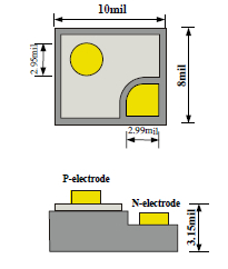
Teknik pertumbuhan - MOCVD
Substrat bahan: Sapphire substrat (Al2O3)
Substrat Pengaliran: Penebat
Substrat Orientation: c-Plane (0001) 0.2 ° ± 0.1
Diameter: 50.8mm ± 0.15 mm
Ketebalan: 430μm ± 20μm
Panjang gelombang: 395nm-405nm
2. Physical Parameters of InGaN/GaN Structure on Sapphire
|
struktur
|
InGaN / struktur Gan pada nilam EPI wafer
|
|
PN elektrod
|
Au
|
|
saiz cip
|
8mil × 10mil (200 ± 5μm × 250 × 5μm)
|
|
tebal serpihan
|
3.15mil (80 ± 5μm)
|
|
saiz pad
|
2.95mil (75 ± 5μm)
|
3. Photoelectric Parameters Based on GaN LED Wafer(IF= 20mA, Tc = 22 ℃)
|
parameter
|
simbol
|
Keadaan
|
Min.value
|
nilai tipikal
|
Max.value
|
|
Mengemukakan voltan (V)
|
VF
|
IF= 20mA
|
2.8
|
3.2
|
3.8
|
|
Songsang semasa (A) jika
|
IR
|
VR= 5V
|
0
|
≤0.1
|
1
|
|
julat panjang gelombang (nm)
|
λP
|
IF= 20mA
|
370
|
400
|
420
|
|
keamatan bercahaya (mw)
|
IV
|
IF= 20mA
|
0.1
|
15
|
25
|
|
Lebar setengah gelombang (nm)
|
Δλ
|
IF= 20mA
|
≤30
|
||
|
maksimum semasa (mA)
|
IMAX
|
DC
|
30
|
||
4. About UV LED Market
According to industry sources, the UV LED market is projected to make exponential growth at an annual average rate of 43 percent from about 47 billion won last year to 280 billion won in 2017. At the same time, the UV LED penetration ratio in the conventional UV Lamp market is expected to grow from 12.7 percent last year to 34.7 percent in 2017.
Ultraviolet means shorter wavelength light that measures about 100 to 400 nanometers, shorter than that of visible rays. Depending on wavelength band, UV provides such functions as sterilization, purification, and Curing (consolidation of liquid state material). It also has diverse areas of applications, including medicine, surface coating and printing. In the future, its applications will likely further expand to include the environment industry, including purification of waste water.
5. About UV LED
UV LED adalah peranti ray pemancar ultraviolet, dan merupakan sumber pencahayaan yang menggunakan LED, sebatian semikonduktor, sebagai ganti lampu merkuri. Dalam perjalanan pengeluaran LED, UV LED boleh direka untuk hanya memancarkan panjang gelombang berkesan diperlukan untuk kegunaan masing-masing, termasuk ubat-ubatan, peralatan rumah dan Pengawetan salutan.
Sebaliknya, UV LED menimbulkan halangan teknologi yang sangat tinggi kerana masalah dalam membentuk lapisan yg berhubung dgn cahaya yang membentangkan sinar ultraviolet. harga yang tinggi dan kuasa optik rendah UV LED kerana halangan teknologi sebelum ini menjadi penghalang kepada perkembangan pasaran.
Beberapa daripada banyak aplikasi UV-LED sekarang disokong kerana peningkatan ini dalam teknologi LED adalah udara, permukaan dan pensterilan air (yg memadam rembasan penyakit), pengesanan racun perosak, membekalkan UVB untuk pertumbuhan tumbuhan yang optimum, pengawetan UV dengan rumusan menyembuhkan lebih mesra alam, pengesanan palsu, lampu hitam - senarai ini berkembang sebagai teknologi pengeluaran UV-LED terus bertambah baik.
6. FAQ about UV LED Wafer on Sapphire
Q: There are some issues that I need to share them with you.
First of all, the UV LED are on patterned sapphire that makes the laser-liftoff process unreliable.
Second, I have done all the fabrication process for UV LEDs and the emission is not in UV range. Two following processes are generally used:
– I have etched 2 um from topside for n-contact and the p-contact is Ni/Au (15/15 nm).
– I have transferred them on other substrate and the LED’s backside is n-contact.
Actually, the processes are working very well with blue LEDs. In case of UV LEDs it is very hard to get UV light. Would you please consider helping me to find the problem?
A: We think it should be done like this: it should be plane etching 1.4um rather than vertical etching, and then do n electrode. But your vertical etching is for what? Vertical results difficult in the laser stripping and bonding, and the underlying structure is not the same, stripping process should match the bottom, do not know your stripping process is for what, you should need to adjust the laser power, AlGaN bad peeling.
Untuk maklumat lanjut, sila hubungi kami e-mel divictorchan@powerwaywafer.com dan powerwaymaterial@gmail.com.