By analyzing the MOSFET, it is known that the switch can be realized by controlling the change of the PN junction.
| Field effect transistor | Type | Name | Principle |
| FET | JFET | Junction | PN junction |
| MOSFET | Metal oxide semiconductor | ||
| MESFET | Metal semiconductor |
Schottky junction |
|
| MODFET | Modulation doping | ||
| HEMT | High electron mobility |
In fact, a Schottky junction can be realized through another structure.
Definitions of Junctions
Starting from the concept of junction, junction is the contact area of the two materials A and B.
PN junction is a space charge area formed at the interface. Using different doping processes, the P-type semiconductor and the N-type semiconductor are fabricated on the same semiconductor substrate (usually silicon carbide substrate or germanium) through diffusion. The electrons of the N-type semiconductor diffuse into the P-type semiconductor filled with holes; the P-type semiconductor is transformed into a semi-insulator in this area, and the N-type semiconductor is transformed into a semi-insulator. There is an electric field from the N-type semiconductor to the P-type semiconductor.
Schottky junction is the contact area between metal and N-type semiconductor. The electrons of the N-type semiconductor diffuse into the free electron gas of the metal with a low energy level. The metal in this region is transformed into an N-type semiconductor, and the N-type semiconductor is transformed into a P-type semiconductor; there is an electric field from the N-type semiconductor to the metal.
That is, by changing the gate of the MOSFET from metal + oxide + semiconductor to metal + N-type semiconductor, a MESFET (Metal-Semiconductor FET) is made.
MESFET is divided into two types:
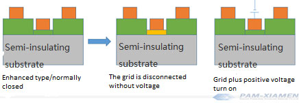
1. Normally open/enhanced type: If the N-type semiconductor is very thick, the gate is turned on from the source to the drain when no voltage is applied, just as a switch is open at the beginning.

2. Normally closed/depleted type: If the N-type semiconductor is very thin, the gate is blocked from the source to the drain when no voltage is applied. In other words, a switch is closed at the beginning.
Reasons for Choosing Semi-insulating Substrate
Thus, why choose a semi-insulating substrate? Because if it is a conductive substrate, the structure will always be on, unable to achieve switching control; and the semi-insulating substrate can reduce parasitic capacitance. Generally speaking, the N-type semiconductor is gallium arsenide, and the gallium arsenide semi-insulating substrate will be selected; the N-type semiconductor is gallium nitride, and the choice of substrate will be SiC semi-insulating substrate, GaN semi-insulating substrate, etc. Semi-insulating silicon carbide is useful in this regard.
So why is the N-type semiconductor emphasized in the structure? Because the electron mobility is greater than the hole mobility, a faster migration can be achieved. This is also the reason for choosing Schottky junction.
To further improve the migration rate, a semi-insulating-semi-insulating heterojunction should be fabricated in the structure.
Modulation of AlxGa1-xAs/GaAs heterojunction or AlxGa1-xN/GaN heterojunction formed by doping metal aluminum Al: the contact area between semi-insulator and semi-insulator.
Since the energy of the Al-doped region is low, the electrons in the undoped region are attracted to the contact surface, which is the two-dimensional electron gas.
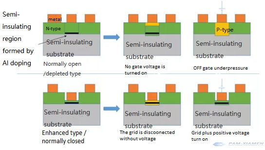
The migration rate of these electrons has been improved. This structure is called MODFET (Modulation-Doped FET) or HEMT (High Electron Mobility Transistor).

For more information, please contact us email at victorchan@powerwaywafer.com and powerwaymaterial@gmail.com.