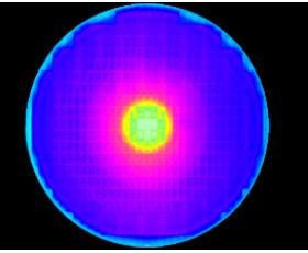
PAM-XIAMEN can offer 6 inch N-type GaAs wafer. Gallium arsenide is a second-generation semiconductor material with excellent performance. Gallium arsenide belongs to the second-generation semiconductors, which has far superior frequency, power and withstand voltage performance than the first-generation silicon semiconductors. According to different resistance, GaAs materials can be divided into semiconductor type and semi-insulating type. Semi-insulating gallium arsenide substrate is mainly used to make PA components in mobile phones because of its high resistivity and good high-frequency performance. Gallium arsenide n type semiconductor is mainly used in optoelectronic devices, like LEDs, VCSELs (vertical cavity surface emitting lasers), etc. The specifications of N-type GaAs wafer are as follows:

1. Specifications of N-type GaAs Wafer
Item 1:
PAM-210406-GAAS
| Parameter | Customer’s Requirements | Guaranteed/Actual Values | UOM | ||
| Growth Method: | VGF | VGF | |||
| Conduct Type: | S-C-N | S-C-N | |||
| Dopant: | GaAs-Si | GaAs-Si | |||
| Diameter: | 150.0±0.3 | 150.0±0.3 | mm | ||
| Orientation: | (100)15°±0.5° off toward (011) | (100)15°±0.5° off toward (011) | |||
| Notch orientation: | [010]±2° | [010]±2° | |||
| NOTCH Depth: | (1-1.25) mm 89°-95° | (1-1.25) mm 89°-95° | |||
| lngot CC: | Min:0.4 E18 | Max:3.5 E18 | Min:0.4 E18 | Max:0.9 E18 | /cm3 |
| Resistivity: | N/A | N/A | Ω*cm | ||
| Mobility: | N/A | N/A | cm2/V-s | ||
| EPD: | Max:5000 | Min:200 | Max:500 | /cm2 | |
| Thickness:: | 550±25 | 550±25 | um | ||
| Edge Rounding: | 0.25 | 0.25 | mmR | ||
| laser Marking: | Back side | Back side | |||
| TTV: | Max;10 | Max:10 | um | ||
| TIR: | Max:10 | Max:10 | um | ||
| Bow: | Max;10 | Max:10 | um | ||
| Warp: | Max:10 | Max:10 | um | ||
| Surface Finish–front: | Polished | Polished | |||
| Surface Finish-back: | Polished | Polished | |||
| Epi-Ready: | Yes | Yes | |||
Item 2:
PAM-210412-GAAS
| Parameter | Customer’s Requirements | Guaranteed/Actual Values | UOM | ||
| Growth Method: | VGF | VGF | |||
| Conduct Type: | S-C-N | S-C-N | |||
| Dopant: | GaAs-Si | GaAs-Si | |||
| Diameter: | 150.0±0.3 | 150.0±0.3 | mm | ||
| Orientation: | (100)±0.5° off toward (011) | (100)±0.5° off toward (011) | |||
| Notch orientation: | [010]±2° | [010]±2° | |||
| NOTCH Depth: | (1-1.25) mm 89°-95° | (1-1.25) mm 89°-95° | |||
| lngot CC: | Min:0.4 E18 | Max:3.5 E18 | Min:0.4 E18 | Max:0.9 E18 | /cm3 |
| Resistivity: | N/A | N/A | Ω*cm | ||
| Mobility: | N/A | N/A | cm2/V-s | ||
| EPD: | Max:5000 | Min:200 | Max:500 | /cm2 | |
| Thickness:: | 625±25 | 625±25 | um | ||
| Edge Rounding: | 0.25 | 0.25 | mmR | ||
| laser Marking: | Back side | Back side | |||
| TTV: | Max;10 | Max:10 | um | ||
| TIR: | Max:10 | Max:10 | um | ||
| Bow: | Max;10 | Max:10 | um | ||
| Warp: | Max:10 | Max:10 | um | ||
| Surface Finish–front: | Polished | Polished | |||
| Surface Finish-back: | Polished | Polished | |||
| Epi-Ready: | Yes | Yes | |||
Item 3: Gallium Arsenide Substrates Doped with Silicon (N-type)
method of growing the initial single crystal gallium arsenide = VGF (vertical gradient freeze)
Crystallographic orientation of the substrate surface = in the (100) direction
Accuracy of orientation of the substrate surface = +/- 0.5 deg.
Silicon doping
Carrier concentration from 1 * 10 (18) cm-3 to 4 * 10 (18) cm-3
Surface density of defects, controlled by the number of etch pit density (EPD) = no more than 500 cm-2
Diameter 50.8 + \ – 0.4mm
Thickness 350 + \ – 25 microns
SEMI-E / J Base cut Orientation
The direction of the main chamfer corresponds to (0-1-1) +/- 0.50
Main chamfer length 17 +/- 1mm
The direction given by the additional chamfer corresponds to (0-11)
Face side = polished, epi-ready
Back side = polished
Packaging = individual container for each substrate, packed in a metallized polyethylene bag filled with an inert gas
2. Adavantages and Applications N-type GaAs Substrate
Due to the characteristics of RF front-end devices, including high voltage resistance, high temperature resistance, and high frequency use, there is a high demand in the 4G and 5G era. Traditional Si devices, such as HBT and CMOS, can not meet the requirements. Manufacturers are gradually turning their attention to n-type doping GaAs wafer. N-type GaAs ohmic contact compound semiconductors have higher electron mobility than Si devices, and have the characteristics of anti-interference, low noise and high voltage resistance. Therefore, N-type GaAs wafer are particularly suitable for high-frequency transmission in wireless communications.
3. FAQ
Q1:Is there any GaAs wafter with lower EPD, such as lower than 500 or 1000?
A: Yes, GaAs, n type/Si doping 3″ or 4″ diameter (100) orientation doping level 0.4-4E18 EPD<500.
Q2: Is there lower doping GaAs wafer or narrow down the doping level to the order of e17cc?
A: Please note the doping concentration is constant, we can not change it.
For more information, please contact us email at victorchan@powerwaywafer.com and powerwaymaterial@gmail.com.

