PAM-XIAMEN, one of leading nanofabrication companies, has formed a compatible management system of multi-material, multi-user, multi-device, multi-process after years of exploration. The details as follows:
* Multi-Material
We can process multiple materials: Si, III-V semiconductor, glass, ceramic;
– Can process wafers of 6 inches and below, compatible with irregular small pieces;
– Can process various film growth and ion source implantation.
* Multi-Party Users
We offer nanomanufacturing services for the users, including: R&D projects for corporate users, topics of universities and research institutes, OEM processing users and equipment and consumables R&D project.
* Multiple Devices
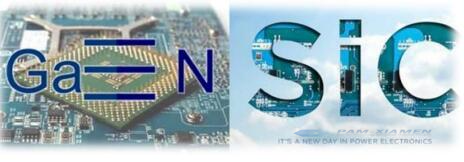
The nanofabrication from PAM-XIAMEN’s wafer foundry service can be for the devices, such as Si MEMS device, GaAs optoelectronic dvices and GaN power electronic devices.
* Multiple Processes
We have a variety of nanofabrication manufacturing technologies, like complete processing technology from front to back, multiple methods (optics, mechanics, acoustics) for test and characterization, multi-physics simulation software and so on.
In addition, we possess strong hardware and equipment capabilities, more details please see below:
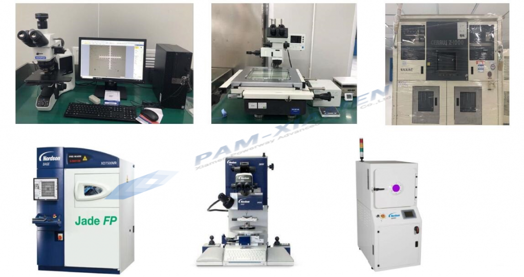
1. Ultra-Clean Environment in Nanofabrication Lab
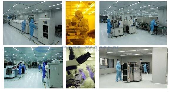
Nanofabrication Lab – Ultra-Clean Environment
2. Nanofab Equipment Overview
|
Overview of processing platform equipment |
||||
| Process | Device model | |||
| DB | ASM 832i(3 units) | ESEC 2100hs | ESEC 2007 | – |
| WB | K&S ConnX Elite | K&S ICONNPLUs | K&S ICONN LA (10 units) | OE 360CHD |
| Tinning (Spraying Glue) | Mingseal CS-600(4 units) | – | – | – |
| Semiconductor SMT | DEK Printing Machine | Samsung Mounter | BTU Reflow Oven | MaGICray AOI |
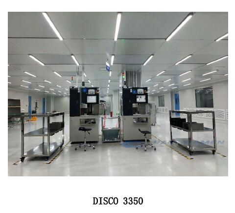
| Back End | DISCO 3350(2 units) | Han’s Marking Machine | ASM Molding Machine | MARCH AP1000 |
| Photolithography | BG-406/6S Double-sided Exposure Machine | Hefei Zhenping HMDS | MYCEO Spreading Machine | – |
| Inspection and Others | Dage4000 | Dage 7500VR-Xay | Olympus STM7 | Olympa BX53M |
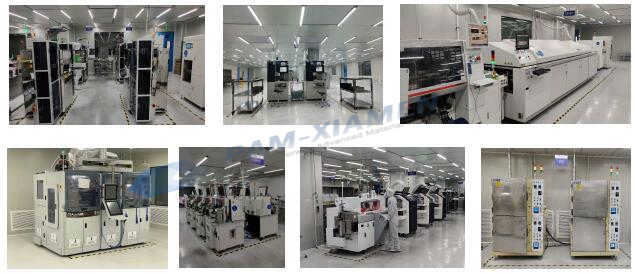
Nanofabrication Equipment
3. Nanofabrication Facility in the Yellow Zone
The accuracy of the lithography machine: front alignment ±1um, back alignment ±4um;
Adapt to product size: compatible with 6 inches and below;
Equipment type: contact lithography;
Exposure light source: UV365, 500W ultra-high pressure mercury lamp;
Exposure resolution: 1.5um (gel thickness ≤ 1um, positive glue, vacuum contact);
Yellow light area configuration: 100-level workshop, equipped with a series of processes such as HMDS, homogenizing, pre-baking, post-baking, and photolithography.
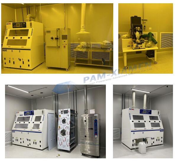
Nanofabrication Facility in the Yellow Zone
4. Dicing Equipment
Dicing is the process of separating wafers (Chip) with circuit patterns made through semiconductor pre-processes into small chips (Die) in a specific method.
Wafer size: 2-8 inches;
Scribing method: grinding wheel knife scribing;
Scribing materials: Si, GaN, GaAs, InP, sapphire, glass, ceramics, packaging substrates, etc.;
Spindle speed: 6000rpm
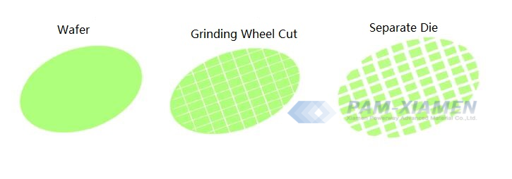
Dicing Process Diagram
Dicing Equipment
5. Surface Mount Technology Equipment
Surface mount technology (SMT) is to package the chip on the lead frame in order to realize the electrical connection to the chip and improve stress, the heat dissipation performance and reliability.
Solder: conductive glue, silver paste, gold/tin solder, In solder, gold, copper, etc.;
Welding accuracy: ASM (±20um), ESEC (±25um);
Chip size: 0.15*0.15mm~20*20mm;
Wafer size: 12 inches and below are compatible
Welding method: hot-press bonding, eutectic welding, flip-chip welding, gluing process, etc.
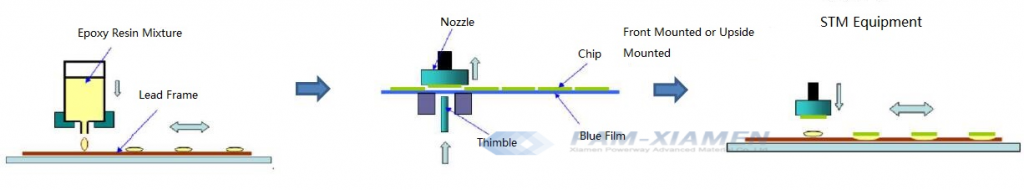
SMT Process
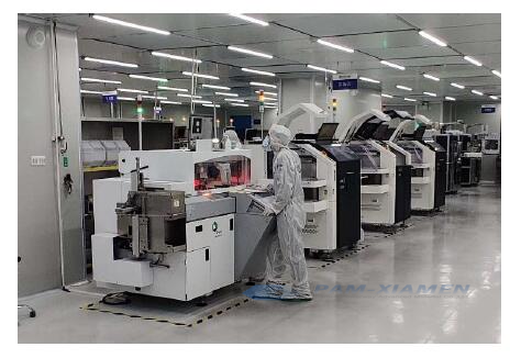
SMT Equipment
6. Wire Bonding Equipment
Wire bonding is to use metal wires to interconnect the chip’s I/O end (inner lead terminal) with the corresponding package pin or wiring lands (outer lead terminal) on the substrate to achieve a solid phase welding process.
Metal wire material: Au wire, Al wire, Cu wire;
Wire diameter: tens of microns to hundreds of microns;
The shape of the key bonding tool: spherical bonding and wedge bonding;
Bonding accuracy: ±3um (up to ±2um)
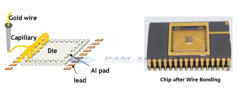
Wire Bonding Process Diagram
Wire Bonding Equipment
7. Nanofabrication Process Capability—Special Process
Actual products fabricated by nanofabrication process:
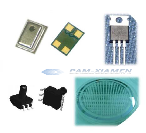
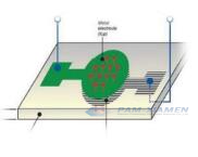
Here are examples showing nanofabrication for optics, biological applications:
GaN & SiC materials and devices:
MEMS quantum chip and packaging:
FBAR filter TC-SAW filter:
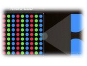
MicroLED:
Neuromorphic calculation of spin-like brain devices:

In the development of the past few decades, nanofabrication technology has promoted the rapid development of integrated circuits and realized the high integration of devices. The main difference between nano-processing technology and traditional processing technology is that the size of the device structure formed by this process is on the order of nanometers. Following are brief nanofabrication techniques and principles. There are two types of nanofabrication:
- One is the top-down nanofabrication, that is, complex microstructures are formed layer by layer on the surface of a flat substrate. It can also be understood as specific processing based on existing materials to realize nanostructures and devices. Currently, photolithography, nano-imprinting, and probe technology belong to nanofabrication techniques;
- The other is the bottom-up nanofabrication, which relies on the molecular self-assembly process, which can build nanostructures from the molecular level. This type of processing method is to obtain patterns through molecular growth without the existence of basic structures or materials.

For more information, please contact us email at victorchan@powerwaywafer.com and powerwaymaterial@gmail.com.