Photolithography chrome masks are for sale. According to the different substrate materials, it can be divided into quartz mask, soda mask and others (including relief plate, film), etc. Among them, the photomask on quartz substrate and soda lime are commonly used lithography masks in universities and research institutes. More about the specifications from PAM-XIAMEN please see as follows:
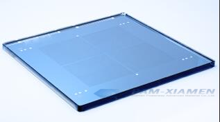
No.1 Chrome Mask Blank PAM191218-MASKS
|
Mask Substrate Specifications |
|
| Material | soda lime |
| Dimension | 3″x3″ |
| Thickness | 0.060” ±0.004” |
| Flatness | ≤ 15u |
| Defects | None |
| Chrome Metallisation Specifications | |
| Chrome Film thickness | 1100A±10% |
| Optical Density @ 530 nm | 2.8±0.2 |
| Mask Plate grade | |
| Pin hole | >5um none,1-5u 0.3/ square inch |
| Resist Specifications | |
| Resist | AZ1500 |
| Resist thickness | 5300A±150A |
| Defects | None |
Mark:
Chrome Mask plates are coated with photo resist. These mask plates are used for making patterns having minimum features down to 0.5 micron using LASER lithography and wet/dry etching hence.
No.2 Photolithography Mask PAM190702-MASKL
| Material | 5 inch Lithography Mask |
| Requirements | Photomask for stepper ( model: 5009)
Model of the lithography machine: ASML PA5000/50 Scale: 5:1 |
| Graphic quality index requirements | |
| Graphic accuracy | 100% |
| CD | 2um |
| CD Tolerance | <0.5um |
| Defect Density | ≤1 pc |
| Engraving Tolerance | <0.5um |
No. 3 Photolithography Mask Patterned with Chrome PAM190621-MASKL
No. 3-1 Photolithography Mask Design and Printing 4”
Mask size: 4” x 4” square
Mask material: Quartz
Pattern material: Chrome
Service to include pattern design for high-electron mobility transistor (HEMT) fabrication process (6 patterns), and transmission line measurement (TLM) for specific contact resistance analysis (2 patterns)
4 pattern design on 1 mask (each at 1/4 area of the mask) – total 8 designs
No. 3-2 Photolithography Mask Design and Printing 5”
Mask size: 5” x 5” square
Mask material: Quartz
Pattern material: Chrome
Service to include pattern design for patterned-sapphire substrate (PSS)
4 pattern designs on 1 mask (each at 1/4 area of the mask)
Please note: Technical parameters of the above 2 items meet the following requirements:
| Mask Sizes (mm) | Minimum Seam & Line Width | Seam Accuracy | Mark |
| 101.6*101.6*2.3 | 3um≤W≤5um | ±0.3um | Quartz material |
| 127.0*127.0*2.3 | 3um≤W≤5um | ±0.3um | Quartz material |
| 101.6*101.6*3.0 | 3um≤W≤5um | ±0.3um | Quartz material |
| 127.0*127.0*3.0 | 3um≤W≤5um | ±0.3um | Quartz material |
No. 4 Phase Mask PAM190717-MASKQ
Pitch: 1095.8nm
Size: 25mm x 3mm
Illumination wavelength 248nm
Substrate Size:35*17.2mm
Thickness of Phase Mask: 1/4 inch (6.35mm)
No. 5 Uniform Phase Mask PAM190821-MASKJ
Uniform Phase Mask for 1575 nm Bragg Grating
Grating period: 1088 nm
Grating period accuracy and uniformity: +/- 0.01 nm
Grating size: 10 mm x 10 mm
Substrate size: 30 mm x 25 mm
Optimized for 248 nm unpolarized illumination
0. order: < 3%

For more information, please contact us email at victorchan@powerwaywafer.com and powerwaymaterial@gmail.com.