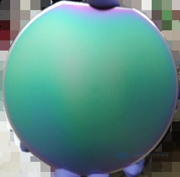
Below is the regular standard specification of Polycrystalline back sealed polished wafer, please kindly note in this size, normally notch is used, rather than flat.

Si Wafer with back seal poly+SiO2
1. Polycrystalline Back Sealed Silicon Wafer Specification
| Parameter | Unit | PAM210305-SI | |||
| Grade | — | Polycrystalline back sealed polished wafer | |||
| General Characteristics | — | — | |||
| Growth Method | — | CZ | |||
| Diameter | mm | 200±0.2 | |||
| Type | — | N | |||
| Crystal Orientation | — | <100>±0.5 | |||
| Dopant | — | AS | |||
| Electrical Characteristics | — | — | |||
| Resistivity | Ω•cm | 0.002-0.004 | |||
| RRG 1 C-1/2R MAX | % | / | |||
| RRG 2 C-6mm MAX | % | ≤8 | |||
| Life time | msec | / | |||
| Chemical Characteristics | — | — | |||
| Oxygen | PPMA | / | |||
| ORG | % | / | |||
| Carbon | PPMA | / | |||
| Bulk metal | #/cm3 | / | |||
| Surface metal | #/cm2 | ≤5E10(Na,K,Al,Ni,Ca;Cu,Zn,Cr,Fe) | |||
| Structural Characteristics | — | — | |||
| Dislocation | #/cm2 | None | |||
| OISF | #/cm2 | / | |||
| Mechanical Characteristics | — | — | |||
| Slicing Off Orientation | Degree | 0±0.5 | |||
| Primary Flat Location | Degree | NONE | |||
| Primary Flat Length | mm | NONE | |||
| Secondary Flat Location | Degree | NONE | |||
| Secondary Flat Length | mm | NONE | |||
| Thickness | mm | 725.0±20.0 | |||
| TTV | mm | ≦4 | |||
| Bow | mm | ≦50(3PT) | |||
| Warp | mm | ≦50(3PT) | |||
| TIR | mm | ≦3 | |||
| STIR | mm | SFQR ≦0.4(25mm*25mm) | |||
| Edge Profile | — | 22±2° X1=70-230µm;X2=500-600µm;X3>0 | |||
| Laser Marking | — | NONE | |||
| Surface Characteristics | — | — | |||
| Front side | Particle | mm | ≦10(≥0.3μm), ≦15(≥0.2μm), ≦50(≥0.16μm) | ||
| #/SL | |||||
| Backside | BSD | — | NO BSD | ||
| Etched | acid | Alkali | — | Etched | |
| Polished | — | / | |||
| Poly | AP | LP | Å | 8000±800(first) | |
| Oxide | AP | LP | Å | 4500±500(next)(WJ1500) | |
| Edge Exclusion | mm | <0.6 | |||
| Customer Part No. | — | / | |||
| Package | — | Standard packing | |||
2. What Is Back Seal of Silicon Wafer?
Epitaxial silicon wafer is the key basic material of the semiconductor integrated circuit industry, and most of the production processes of large-scale integrated circuits use epitaxial silicon wafers. Epitaxial silicon wafers can be obtained by epitaxial growth of silicon wafers, but there will inevitably be self-doping in the process. One possible reason for the self-doping phenomenon is that under the high temperature environment of epitaxial growth of silicon wafers, dopant atoms such as boron or phosphorus contained in the silicon wafer diffuse out and pass through the backside of the silicon wafer into the reaction gas for epitaxial growth is deposited into the epitaxial layer of the silicon wafer. When the above-mentioned dopant atoms are deposited in the epitaxial layer of the silicon wafer, the resistivity drift will be caused, which will seriously affect the quality of the epitaxial wafer. Therefore, back sealed technology is proposed.
Silicon wafer back sealing is a commonly used method to prevent self-doping phenomenon. This technology refers to depositing a layer of silicon dioxide or polysilicon, silicon nitride and other insulating films on the back of the silicon wafer to prevent the above-mentioned dopant atoms from passing through the back of the silicon wafer and entering the reaction gas to seal the dopant atoms. It can effectively suppress self-doping, reduce the influence on resistivity, and improve the quality of epitaxial silicon wafers.
For more information, please contact us email at victorchan@powerwaywafer.com and powerwaymaterial@gmail.com

