PSA-01 is a portable nuclear spectrum acquisition instrument, which integrates main amplifier,multi-channel pulse analyzer and high-voltage. Its gain, high-voltage and shaping time are adjustable. With upper computer software, it can acquit nuclear spectrum, analyzing, processing and storage data. Its built-in Li-battery could charge more than 10,000 times. Cooperate with our CZT detector, it can build a platform sufficiently for X/γ-ray spectrum acquisition.
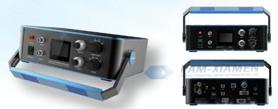
Specification of Portable Diagnostic Spectrum Analyzer
| Input range | 0~100kHz |
| Multi-channel input range | 0~4V |
| Gain range | 1.5~10 |
| shaping time range | 0.29us~38us |
| High voltage output | DC 0~±2000V |
| Low voltage output | DC±12V |
| Continuously working time | 8 hours |
| Communication methods | USB2.0, Ethernet |
| Dimensions | 350×330×150mm3 |
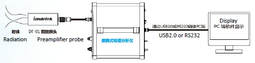
Operating principle

For more information, please contact us email at victorchan@powerwaywafer.com and powerwaymaterial@gmail.com.