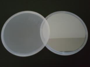
GaAs / AlGaAs / GaAs epi wafer in the diameter of 2” or 4” is available. This GaAs epitaxial wafer is applicable for semiconductor microwave devices and microwave monolithic integrated circuits. Here comes the typical structure of gallium arsenide epi wafer, please see below:
1. GaAs Wafer Epitaxial Structures
Structure 1:
2”GaAs/AlGaAs/GaAs epi wafer
| S.No | Parameters | Specifications |
| 1 | GaAs substrate layer thickness | 500μm |
| 2 | layer thickness | 2μm |
| 3 | GaAs top layer thickness | 220 nm |
| 4 | Mole fraction of Al (x) | 0.7 |
| 5 | Doping level | Intrinsic |
Structure 2:
2DEG GaAs/AlGaAs epi wafer PAM-230403-GAAS-HEMT(universal)
| Structure | Composition | Thickness(nm) |
| Cap | GaAs | 5 |
| Doping carrier | AlGaAs, 1.4E18/cm3 | – |
| spacer | AlGaAs | – |
| channel | GaAs | – |
| SL | GaAs/AlGaAs | – |
| buffer | GaAs | 200 |
| Sub | GaAs | – |
Structure 3:
PAM181206-ALGAAS
| Layer Structure | Composition | Thickness |
| Mesa | GaAs:Si | – |
| AlGaAs:Si | 55nm | |
| AlGaAs | – | |
| GaAs | 110nm | |
| Beam | GaAs | – |
| GaAs/AlGaAs SL | – | |
| Sacrificial Layer | AlGaAs | – |
| Substrate | GaAs | – |
Structure 4:
4″diameter AlGaAs/GaAs Wafer
The structure (top to bottom) PAM-190605-ALGAAS:
GaAs (10 nm)
AlGaAs (30 nm) with 30% Al and 70% Ga, doped at 1E18 cm^-3
Undoped AlGaAs (15 nm) (30% Al and 70% Ga)
GaAs (500 nm)
GaAs substrate
Remark: mobility and 2DEG concentration can be tested if necessary
Structure 5:
GaAs/AlGaAs epi stack wafers PAM-190711-ALGAAS
150nm of GaAs layer Standard error 3%
5um Al0.8Ga0.2As layer
2” GaAs substrate (backside polished)~ 330um
Expanation: the epi stack grows on top of GaAs substrate and contains 5 um of Al0.8Ga0.2As sacrificial layer and 150nm of GaAs layer on top of the sacrificial layer for the MBE-grown wafers.
2. GaAs Epi Wafer Industrial Standard Requirements
This standards specify the grades, requirements, quality assurance regulations and delivery preparations for semiconductor microwave devices and gallium arsenide epitaxial wafers for microwave monolithic integrated circuits.
2.1 Parameters of Epi Wafer of GaAs
The GaAs epitaxial technical parameters should meet the requirements of Table 1;
The GaAs epi wafer dimensions are conform with the requirements in the Figure 1 and Table 2.
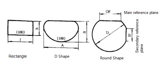
Table 1 Technical Parameters of GaAs Epiwafer
| Applications | Microwave Monolithic Integrated Circuit | Microwave Field Effect Transistor | Microwave Diode | |||||||||
| Power | Low noise | Power | Low noise | Beam lead mixer | Schottky Barrier Tube | Power Schottky Barrier Tube | Gunn tube | Varactor | Hypermutation junction varactor | |||
| Epitaxial Wafer Structure | Epitaxial layer (3) | n+ | n+ | n+1) | n+1) | – | – | – | n+ | – | – | |
| Epitaxial layer (2) | n | n | n | n | n | n | – | n | – | – | ||
| Epitaxial layer (1) | n- | n- | n- | n- | n+ | n+ | n | n+ | n | △n | ||
| Substrate | S.I | S.I | S.I | S.I | n++ | n++ | n++ | n++ | n++ | |||
| Epitaxial Layer | (3) | Carrier concentration (cm-3) | ≥1 x 10 18 | ≥1 x 10 18 | – | – | – | ≥1 x 10 18 | – | – | ||
| Thickness (um) | 0.1~0.4 | – | – | – | – | – | – | |||||
| Mobility at Room Temperature (cm2/V.s) | – | – | – | – | – | – | – | – | – | – | ||
| (2) | Carrier concentration (cm-3) | 1.5 x 10¹⁷~2 x 10¹⁷ | 2 x 10¹⁷~2.5 x 10¹⁷ | 5 x 10¹⁶~2 x 10¹⁷ | 1.0 x 10¹⁷~3 x 10¹⁷ | 8 x 10¹⁵~2 x 10¹⁷ | – | 4 x 10¹⁴~1.5 x 10¹⁶ | – | – | ||
| Thickness (um) | 0.2~0.5 | 0.2~0.5 | 0.2~0.4 | 0.3~0.5 | – | 30~1.5 | – | – | ||||
| Mobility at Room Temperature (cm2/V.s) | >3000 | >3000 | >3000 | >3000 | – | 7000~4000 | – | – | ||||
| (1) | Carrier concentration (cm-3) | <1 x 10¹⁴ | <1 x 10¹⁴ | ≥1 x 10¹⁸ | ≥1 x 10¹⁸ | 5 x 10¹⁴~1 x 10¹⁶ | ≥5 x 10¹⁷ | 4 x 10¹⁵~10 x 1015 | 5 x 10¹⁵~5 x 10¹⁶ | |||
| Thickness (um) | 3~5 | 3~7 | 3~50 | 2~4 | 2~6 | 1~4 | ||||||
| Mobility at Room Temperature (cm2/V.s) | – | – | – | – | – | – | – | – | – | – | ||
| Substrate | Carrier concentration (cm-3) | – | – | – | – | – | ≥1 x 10¹⁸ | |||||
| Resistivity(ohm-cm) | ≥1 x 10⁷ | – | – | – | – | – | ||||||
| Thickness (um) | See table 2 | |||||||||||
| Mobility at Room Temperature (cm2/V.s) | – | – | – | – | – | – | – | – | >1800 | >2200 | ||
| Orientation | (100) | |||||||||||
| Growth Method | LEC, HB | LEC, HB | LEC, HB | LEC, HB | LEC, HB | LEC, HB | HB | HB | – | – | ||
Mark:
* Substrate dopants are negotiated by the demander and the supplier;
* When deviating, deviate 2°±0.5° to the nearest (110) direction.
Table 2 GaAs Epitaxy Dimensions
| Parameters | l | h | A | B | D | OF | IF | Thickness | Smin |
| mm | um | cm2 | |||||||
| Rectangle | ≥10 | ≥10 | – | – | – | – | – | 350~650 | 1.0 |
| ≥15 | ≥10 | – | – | – | – | – | 1.5 | ||
| D Shape | – | – | 51~56 | 40~47 | – | – | – | 350~650 | 18.0 |
| – | – | 63~68 | 50~56 | – | – | – | 27.5 | ||
| Round Shape | – | – | – | – | 40 ± 1 | 12.5±1 | 7 ± 1 | 350~650 | 12.5 |
| – | – | – | – | 50 ± 1 | 16±1 | 7 ± 1 | 19.5 | ||
| – | – | – | – | 76 ± 1 | 22±1 | 12 ± 1 | 550~650 | 45.3 | |
| – | – | – | – | 100 ± 1 | 32.5 ± 1 | 18 ± 1 | 600~650 | 78.5 | |
Mark:
Smin represents the area of the epitaxial wafer of GaAs.
2.2 AlGaAs / GaAs Quantum Structure Wafer Quality
Concentration Uniformity of GaAs Epi Wafers:
The concentration uniformity of the active layer of the GaAs epitaxial wafer should be less than or equal to 10%;
The thickness uniformity of the Iactive layer should be less than or equal to 10%;
The the active layer thickness of GaAs wafer should be less than or equal to 10%.
GaAs Wafer Transition Zone Width:
The width of the transition zone of the indium gallium arsenide epitaxial wafer buffer layer for field effect transistors should not be greater than 0.90umc.
GaAs Epi Wafer Surface quality:
* There should be no contamination on the surface of the AlGaAs / GaAs epitaxial wafer;
* There should be no fog, pitting, scratches, scratches on the GaAs epi wafer on GaAs substrate surface;
* The GaAs epitaxy surface should be smooth and bright;
* If there are special requirements for the surface quality of the GaAs wafer on GaAs film, it should be negotiated by the supplier and the buyer.

For more information, please contact us email at victorchan@powerwaywafer.com and powerwaymaterial@gmail.com.