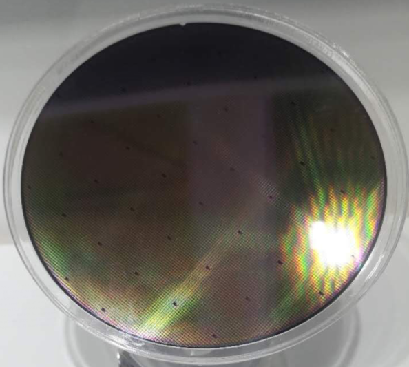
Epi Wafer para diodo laser
O wafer de epitaxia LD baseado em GaAs, que pode gerar emissão estimulada, é amplamente utilizado para fabricar diodo laser, uma vez que as propriedades superiores do wafer epitaxial GaAs tornam o dispositivo um baixo consumo de energia, alta eficiência, longa vida útil e etc. Além do arseneto de gálio LD epi wafer , os materiais semicondutores comumente usados são sulfeto de cádmio (CdS), fosfeto de índio (InP) e sulfeto de zinco (ZnS).
- Descrição
Descrição do produto
Xiamen Powerway Advanced Material Co., Ltd (PAM-XIAMEN), um fornecedor de wafer epitaxial LD, concentra-se em wafers epi de diodo laser baseados em GaAs e InP cultivados por reatores MOCVD para comunicação de fibra óptica, aplicação industrial e uso para fins especiais. PAM-XIAMEN pode oferecer wafer de epitaxia LD baseado em substrato GaAs para vários campos, como VCSEL, infravermelho, fotodetector e etc. Mais detalhes sobre o material de wafer de epitaxia LD, consulte a tabela abaixo:
| substrato material | Capacidade de materiais | Comprimento de onda | Aplicação |
| GaAs | GaAs / GalnP / AlGaInP / GaInP | 635nm | |
| Epi-wafer baseado em GaAs | 650nm | Laser emissor de superfície de cavidade vertical (VCSEL) RCLED |
|
| GaAs / GalnP / AlGaInP / GaInP | 660nm | ||
| GaAs / AlGaAs / GalnP / AlGaAs / GaAs | 703nm | ||
| GaAs / GalnP / AlGaInP / GaInP | 780nm | ||
| GaAs / GalnP / AlGaInP / GaInP | 785nm | ||
| Epi-wafer baseado em GaAs | 800-1064nm | LD infravermelho | |
| GaAs / GalnP / AlGaInP / GaInP | 808nm | LD infravermelho | |
| Epi-wafer baseado em GaAs | 850nm | Laser emissor de superfície de cavidade vertical (VCSEL) RCLED |
|
| Epi-wafer baseado em GaAs | <870nm | Fotodetector | |
| Epi-wafer baseado em GaAs | 850-1100nm | Laser emissor de superfície de cavidade vertical (VCSEL) RCLED |
|
| GaAs / AlGaAs / GaInAs / AlGaAs / GaAs | 905nm | ||
| GaAs / AlGaAs / InGaAs / AlGaAs / GaAs | 950nm | ||
| Epi-wafer baseado em GaAs | 980nm | LD infravermelho | |
| Epi-wafer baseado em InP | 1250-1600nm | Detector fotográfico de avalanche | |
| Epi-wafer baseado em GaAs | 1250-1600nm/>2,0um (Camada absorvente InGaAs) |
Fotodetector | |
| Epi-wafer baseado em GaAs | 1250-1600nm/<1,4μm (Camada absorvente InGaAsP) |
Fotodetector | |
| Epi-wafer baseado em InP | 1270-1630nm | Laser DFB | |
| Substrato GaAsP / GaAs / GaAs | 1300nm | ||
| Epi-wafer baseado em InP | 1310nm | Laser FP | |
| Substrato GaAsP / GaAs / GaAs | 1550nm | Laser FP | |
| 1654 nm | |||
| Epi-wafer baseado em InP | 1900nm | Laser FP | |
| 2004nm |
Sobre aplicações e mercado de LD Epitaxy Wafer
As aplicações de wafer epitaxia LD baseado em GaAs no campo do laser podem ser divididas em VCSELs e não-VCSELs. As atuais aplicações de epitaxia LD baseadas em GaAs residem principalmente em VCSELs. VCSEL (Laser emissor de superfície de cavidade vertical), baseado em materiais GaAs, é usado principalmente para reconhecimento facial. Espera-se que tenha uma alta taxa de crescimento no futuro. EEL (Edge Emitir Laser) é um dispositivo não VCSEL, usado principalmente na área de lidar automotivo, e espera-se que a demanda aumente com a expansão do mercado de carros sem motorista.
O substrato GaAs usado no campo do laser requer altos indicadores técnicos, e o preço unitário do wafer epitaxial é significativamente maior do que o de outros campos. O futuro espaço de mercado epitaxial de LD pode ser esperado. As aplicações de laser são as mais sensíveis à densidade de deslocamento. Há uma alta exigência para materiais de substrato de GaAs em aplicações de laser. Portanto, o requisito mais alto é apresentado aos fabricantes de wafer epitaxial LD e ao processo de wafer epitaxial LD. Atualmente, o laser semicondutor da banda do infravermelho próximo (760 ~ 1060 nm) baseado no substrato GaAs tem o desenvolvimento mais maduro e a aplicação mais difundida, e já foi comercializado.
Observação:
O governo chinês anunciou novos limites à exportação de materiais de gálio (como GaAs, GaN, Ga2O3, GaP, InGaAs e GaSb) e materiais de germânio usados para fabricar chips semicondutores. A partir de 1º de agosto de 2023, a exportação desses materiais só será permitida se obtivermos uma licença do Ministério do Comércio da China. Espero sua compreensão e cooperação!
Por favor, veja abaixo as especificações detalhadas do wafer epitaxia LD:
Microplaqueta da bolacha do laser de VCSEL
Epi wafers-2 de diodo laser de 808nm
Diodo laser epi wafer de 850 nm
bolacha epi do diodo laser 940nm
Bolacha de laser de alta potência 1060nm
Bolacha de diodo laser de bomba 1460nm
Díodo laser de 2004 nm epi wafer
Epitaxia GaAs com crescimento espesso
Estrutura Epi baseada em GaAs MOCVD cultivada para emissor de luz
Narrow InGaAsP Quantum bem desenvolvido em InP Wafer
Camadas de pontos quânticos InAs no substrato InP
Bolacha Laser FP (Fabry-Perot)
Bolacha Laser em Cascata Quântica
Chips de emissor único
Chip LD de emissor único 755nm @ 8W
-Emissor único LD Chip 808nm @ 8W
Chip LD de emissor único 808nm @ 10W
Chip LD de emissor único 830nm @ 2W
Chip LD de emissor único 880nm @ 8W
Chip LD de emissor único 900 + nm @ 10W
Chip LD de emissor único 900 + nm @ 15W
Chip LD de emissor único 905nm @ 25W
Chip LD de emissor único 1470nm @ 3W
A PAM XIAMEN oferece chip único de laser de alta potência 1470/1550 nm da seguinte forma:
LD Bare Bar
LD Barra Nua para 780nm @ cavidade 2,5mm
LD Barra Nua para 808nm @ cavidade 2mm
LD Barra Nua para 808nm @ cavidade 1,5mm
LD Barra Nua para 880nm @ cavidade 2mm
LD sem folhagem de bar para 940 nm @ 2 milímetros cavidade
LD nua Bar para 940nm @ cavidade 3 milímetros
LD nua Bar para 940nm @ cavidade 4 milímetros
LD sem folhagem de bar para 940 nm @ 2 milímetros cavidade
LD nua Bar para 976nm @ cavidade 4 milímetros