
GaAs Epiwafer
PAM-XIAMEN is manufacturing various types of epi wafer III-V silicon doped n-type semiconductor materials based on Ga, Al, In, As and P grown by MBE or MOCVD. We supply custom GaAs epiwafer structures to meet customer specifications, please contact us for more information.
- Descrição
Descrição do produto
GaAs Epi wafer
As a leading GaAs epi wafer foundry, PAM-XIAMEN are manufacturing various types of epiwafer III-V silicon doped n-type semiconductor materials based on Ga, Al, In, As and P grown by MBE or MOCVD, which make a low gallium arsenide epi wafer defect. We supply custom GaAs epiwafer structures to meet customer specifications, please contact us for more information.
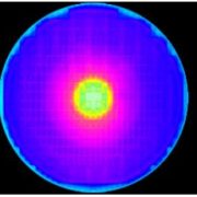
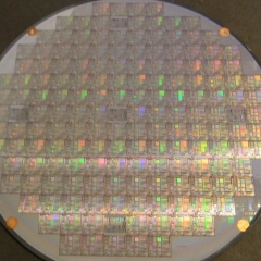
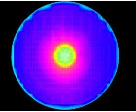
We have numbers of the United States Veeco’s GEN2000, GEN200 large-scale production of epitaxial equipment production line, full set of XRD; PL-Mapping; Surfacescan, and other world-class analysis and testing equipment. The company has more than 12,000 square meters of supporting plant, including world class super-clean semiconductor and a related research and development of the younger generation of clean laboratory facilities.
Specification for all new and featured products of MBE III-V compound semiconductor epitaxial wafer:
| substrato material | Capacidade de materiais | Aplicação |
| GaAs | GaAs baixa temperatura | THz |
| GaAs | GaAs / GaAlAs / GaAs / GaAs | Schottky Diode |
| InP | InGaAs | detector PIN |
| InP | InP / InP / InGaAsP / InP / InGaAs | Laser |
| GaAs | GaAs / AlAs / GaAs | |
| InP | InP / INASP / InGaAs / INASP | |
| GaAs | GaAs / InGaAsN / AlGaAs | |
| / GaAs / AlGaAs | ||
| InP | InP / InGaAs / InP | fotodetectores |
| InP | InP / InGaAs / InP | |
| InP | InP / InGaAs | |
| GaAs | GaAs / InGaP / GaAs / AlInP | Célula solar |
| / InGaP / AlInP / InGaP / AlInP | ||
| GaAs | GaAs / GaInP / GaInAs / GaAs / AlGaAs / GalnP / GalnAs | Célula solar |
| / GalnP / GaAs / AlGaAs / AllnP / GalnP / AllnP / GalnAs | ||
| InP | InP / GaInP | |
| GaAs | GaAs / AlInP | |
| GaAs | GaAs / AlGaAs / GalnP / AlGaAs / GaAs | Laser 703nm |
| GaAs | GaAs / AlGaAs / GaAs | |
| GaAs | GaAs / AlGaAs / GaAs / AlGaAs / GaAs | HEMT |
| GaAs | GaAs / AlAs / GaAs / AlAs / GaAs | mHEMT |
| GaAs | GaAs / DBR / AlGaInP / MQW / AlGaInP / GAP | wafer LED, iluminação de estado sólido |
| GaAs | GaAs / GalnP / AlGaInP / GaInP | 635nm, 660nm, 808nm, 780nm, 785nm, |
| / Substrato GaAsP / GaAs / GaAs | 950nm, 1300nm, 1550nm Laser | |
| GaSb | ALSB / GaInSb / InAs | detector de IR, o PIN de detecção, cemera IR |
| silício | InP ou GaAs em Silicon | Alta velocidade IC / microprocessadores |
| InSb | Berílio dopado InSb | |
| / N dopado InSb / Te dopado InSb / |
Gallium arsenide is currently one of the most important compound semiconductor materials with the highest mature epi wafer technology. GaAs material has the characteristics of large forbidden band width, high electron mobility, direct band gap, high luminous efficiency. Due to all all these epi wafer advantages, GaAs epitaxy is currently the most important material used in the field of optoelectronics. Meanwhile, it is also an important microelectronic material. According to the difference in electrical conductivity, GaAs epi wafer materials can be divided into semi-insulating (SI) GaAs and semiconductor (SC) GaAs.
In the field of epitaxial wafers, the epi wafer market share of RF and laser applications is very large.
Para mais especificação de detalhe, consulte o seguinte:
camada LT-epi GaAs sobre substrato de GaAs
LT GaAs Thin Film for Photodetectors and Photomixers
GaAs Schottky Diodo Epitaxial Wafers
InGaAs / InP bolacha epi para PIN
InGaAsP / InGaAs sobre substratos de InP
InGaAs APD Wafers with High Performance
InGaAsN epitaxialmente em GaAs ou wafers InP
Estrutura para fotodetectores InGaAs
InP / InGaAs / InP bolacha epi
AlGaP / GaAs Epi bolacha por célula solar
Solar Cell Structure Epitaxially Grown on InP Wafer
Growth of GaAsSb / InGaAs Type-II Superlattice
estrutura de camadas de laser 703nm
AlGaAs / GaAs PIN Epitaxial Wafer
1550nm GaInAsP / InP PIN Photodiode Structure
GaAs / AlGaAs / GaAs epi bolacha
Agora vamos listar algumas especificações:
| GaAs HEMT epiwafer, size:2~6inch | ||
| Item | Especificações | Observação |
| Parâmetro | composição de Al / Na composição / A resistência de folha | Entre em contato com o nosso departamento de tecnologia |
| mobilidade Recepção / Concentração 2DEG | ||
| tecnologia de medição | difração de raios-X / corrente Eddy | Entre em contato com o nosso departamento de tecnologia |
| salão Un-contact | ||
| válvula típica | struture dependente | Entre em contato com o nosso departamento de tecnologia |
| 5000 ~ 6500cm2 / V ‡ S / 0,5 ~ 1,0 x 1,012 centímetro-2 | ||
| tolerância padrão | 0,01 ± / ± 3% / nenhum | Entre em contato com o nosso departamento de tecnologia |
| GaAs (arsenieto de gálio) pHEMT epiwafer, size:2~6inch | ||
| Item | Especificações | Observação |
| Parâmetro | composição de Al / Na composição / A resistência de folha | Entre em contato com o nosso departamento de tecnologia |
| mobilidade Recepção / Concentração 2DEG | ||
| tecnologia de medição | difração de raios-X / corrente Eddy | Entre em contato com o nosso departamento de tecnologia |
| salão Un-contact | ||
| válvula típica | struture dependente | Entre em contato com o nosso departamento de tecnologia |
| 5000 ~ 6800cm2 / V ‡ S / 2,0 ~ 3,4 vezes 1,012 centímetro-2 | ||
| tolerância padrão | 0,01 ± / ± 3% / nenhum | Entre em contato com o nosso departamento de tecnologia |
| Remark:GaAs pHEMT: Compared with GaAs HEMT, GaAs PHEMT also incorporates InxGa1-xAs,where InxAs is constrained to x < 0.3 for GaAs-based devices. Structures grown with the same lattice constant as HEMT, but different band gaps are simply referred to as lattice-matched HEMTs. | ||
| GaAs mHEMT epiwafer, size:2~6inch | ||
| Item | Especificações | Observação |
| Parâmetro | Em resistência composição / Folha | Entre em contato com o nosso departamento de tecnologia |
| mobilidade Recepção / Concentração 2DEG | ||
| tecnologia de medição | difração de raios-X / corrente Eddy | Entre em contato com o nosso departamento de tecnologia |
| salão Un-contact | ||
| válvula típica | struture dependente | Entre em contato com o nosso departamento de tecnologia |
| 8000~10000cm2/V ·S/2.0~3.6x 1012cm-2 | ||
| tolerância padrão | ± 3% / nenhum | Entre em contato com o nosso departamento de tecnologia |
| InP HEMT epiwafer, size:2~4inch | ||
| Item | Especificações | Observação |
| Parâmetro | Na resistência Composição / Folha de mobilidade / Salão | Entre em contato com o nosso departamento de tecnologia |
Remark: GaAs(Gallium arsenide) is a compound semiconductor material,a mixture of two elements, gallium (Ga) and arsenic (As). The uses of Gallium arsenide are varied and include being used in LED/LD, field-effect transistors (FETs), and integrated circuits (ICs)
aplicações do dispositivo
RF Switch, Power and low-noise amplifiers, Hall sensor, modulador óptico
estações de telefone celular ou de base: sem fio
Automotive radar, MMIC, RFIC, Comunicações de fibra óptica
GaAs Epi bolacha por LED serie / IR:
A inscrição 1.Config.geral:
1.1 Método Crescimento: MOCVD
1.2 GaAs epi wafer for Wireless Networking
1.3wafer GaAs epi para LED/ IR e LD / PD
2.Epi especificações wafer:
2.1 tamanho da bolacha: 2” de diâmetro
2.2 GaAs Epi Wafer Structure(from top to bottom):
P + GaAs
p-GAP
p-AlGaInP
MQW-AlGaInP
n-AlGaInP
DBR n-ALGaAs / AlAs
Amortecedor
substrato GaAs
Sepcification 3.Chip (Base de Dados em 9mil * fritas 9mil)
3.1 Parâmetro
Chip Tamanho 9mil * 9mil
Espessura 190 ± 10um
diâmetro eléctrodo 90um ± 5um
3.2 caracteres óptico-eléctricos (Ir = 20mA, 22 ℃)
Comprimento de onda de 620 ~ 625nm
tensão direta 1.9 ~ 2.2V
≥10v inversa tensão
Inversa 0-1uA atual
3,3 caracteres intensidade da luz (Ir = 20 mA, 22 ℃)
IV (MCD) 80-140
3.4 Epiwafer avelength
|
Item |
Unidade |
Red |
Amarelo |
Amarelo verde |
Descrição |
|
Comprimento de onda (λD) |
nm |
585615620 ~ 630 |
587 ~ 592 |
568 ~ 573 |
SE = 20 mA |
Métodos de crescimento: MOCVD, MBE
epitaxia = crescimento de película com uma relação cristalográfica entre o filme e o substrato homoepitaxy (autoepitaxy, isoepitaxy) = película e substrato são mesmo material heteroepitaxy = película e substrato são materiais diferentes. Parapara mais informações sobre os métodos de crescimento, por favor, clique no seguinte:https://www.powerwaywafer.com/technology.html
Remark:
The Chinese government has announced new limits on the exportation of Gallium materials (such as GaAs, GaN, Ga2O3, GaP, InGaAs, and GaSb) and Germanium materials used to make semiconductor chips. Starting from August 1, 2023, exporting these materials is only allowed if we obtains a license from the Chinese Ministry of Commerce. Hope for your understanding and cooperation!
InGaAs Epitaxy Sensor / Detector:
Shortwave Infrared InGaAs Sensor
InGaAs/InAlAs Epistucture for Single Photon Detector
Epiwafer for Photonic Integrated Chip:
Você também pode gostar ...
-
Substrato de bolacha SiC
A empresa possui uma linha completa de produção de substrato de wafer de SiC (carboneto de silício) integrando crescimento de cristal, processamento de cristal, processamento de wafer, polimento, limpeza e teste. Hoje em dia fornecemos wafers comerciais de SiC 4H e 6H com semi-isolamento e condutividade no eixo ou fora do eixo, tamanhos disponíveis: 5x5mm2,10x10mm2, 2”,3”,4”, 6” e 8″, rompendo tecnologias-chave como como supressão de defeitos, processamento de cristais de sementes e crescimento rápido, promovendo pesquisa e desenvolvimento básicos relacionados à epitaxia de carboneto de silício, dispositivos, etc.
-
substrato de GaN autoportante
PAM-XIAMEN estabeleceu a tecnologia de fabricação para autoportante (de nitreto de gálio) lâmina de substrato de GaN, que é para UHB-LED e LD. Crescido por tecnologia de hidreto de epitaxia em fase de vapor (HVPE), O nosso substrato de GaN tem baixa densidade de defeitos.
-
Flutuar-Zone Mono-Crystalline Silicon
A PAM-XIAMEN pode oferecer wafer de silício de zona flutuante, que é obtido pelo método Float Zone. As hastes de silício monocristalino são obtidas através do crescimento da zona flutuante e, em seguida, processam as hastes de silício monocristalino em wafers de silício, chamados wafers de silício de zona flutuante. Como a pastilha de silício fundida na zona não está em contato com o cadinho de quartzo durante o processo de silício da zona flutuante, o material de silício está em estado suspenso. Assim, fica menos poluído durante o processo de fusão da zona flutuante do silício. O teor de carbono e o teor de oxigênio são menores, as impurezas são menores e a resistividade é maior. É adequado para a fabricação de dispositivos de energia e certos dispositivos eletrônicos de alta tensão.
-
Ge (germânio) Cristais individuais e bolachas
PAM-XIAMEN oferece wafer de germânio de 2”, 3”, 4” e 6”, que é a abreviação de wafer Ge cultivado pela VGF / LEC. Wafer de germânio tipo P e N levemente dopado também pode ser usado para experimentos de efeito Hall. À temperatura ambiente, o germânio cristalino é quebradiço e tem pouca plasticidade. O germânio possui propriedades semicondutoras. O germânio de alta pureza é dopado com elementos trivalentes (como índio, gálio, boro) para obter semicondutores de germânio do tipo P; e elementos pentavalentes (como antimônio, arsênico e fósforo) são dopados para obter semicondutores de germânio tipo N. O germânio possui boas propriedades semicondutoras, como alta mobilidade de elétrons e alta mobilidade de buracos. -
Fotorresiste de Nanofabricação
PAM-XIAMEN Oferece placa fotorresistente com fotorresistente
-
InP wafer
A PAM-XIAMEN oferece wafer VGF InP (Fosfeto de Índio) com grau principal ou de teste, incluindo baixo teor de dope, tipo N ou semi-isolante. A mobilidade do wafer InP é diferente em diferentes tipos, baixo dopado>=3000cm2/Vs, tipo N>1000 ou 2000cm2V.s (depende da concentração de dopagem diferente), tipo P: 60+/-10 ou 80+/-10cm2 /Vs (depende de diferentes concentrações de dopagem de Zn), e semi-insultuoso> 2.000 cm2/Vs, o EPD do Fosfeto de Índio está abaixo de 500/cm2 normalmente.
-
GaAs (gálio arsenieto) Bolachas
As a leading GaAs substrate supplier, PAM-XIAMEN manufactures Epi-ready GaAs(Gallium Arsenide) Wafer Substrate including semi-conducting n type, semi-conductor C doped and p type with prime grade and dummy grade. The GaAs substrate resistivity depends on dopants, Si doped or Zn doped is (0.001~0.009) ohm.cm, C doped one is >=1E7 ohm.cm. The GaAs wafer crystal orientation should be (100) and (111). For (100) orientation, it can be 2°/6°/15° off. The EPD of GaAs wafer normally is <5000/cm2 for LED or <500/cm2 for LD or microelectronics.
-
CdZnTe (CZT) da bolacha
Cádmio zinco Telluride (CdZnTe ou CZT) é um novo semicondutor, que permite converter a radiação de electrões de forma eficaz, que é utilizado principalmente no infravermelho de película fina epitaxia de substrato, detectores de raios-X e detectores de raios gama de CdZnTe.


Produtos relacionados
-
com base GaN LED epitaxial Wafer
GaN do PAM-XIAMEN (nitreto de gálio) à base de LED bolacha epitaxial é de alto brilho diodos emissores de luz ultra-azul e verde (LED) e diodos laser (LD) de aplicação.
