Silicon carbide has a variety of crystal types, but the silicon crystal structure the market needed is mainly 4H-SiC. So the silicon carbide crystal growth in crystal types is a defect. To a certain extent, it can be distinguished by the naked eye. A more accurate measurement method for testing the silicon carbide crystal distribution is Raman spectroscopy: Raman spectroscopy has characteristics for crystals, and the peak positions of the light emitted by different crystals are different.
1. What is Raman Spectroscopy?
Em 1928, o cientista indiano Raman descobriu o espalhamento Raman no experimento de estudar o espectro de espalhamento do benzeno líquido. A espectroscopia de espalhamento Raman, em termos simples, é que usa um feixe de luz incidente sobre uma substância, a frequência da luz incidente é v, e a frequência da luz espalhada resultante será v, v + Δv1, v-Δv1, v + Δv2, v-Δv2 e assim por diante. Esses Δv1, Δv2, etc. Δv são com características. Em outras palavras, cada substância tem uma certa diferença (posição do pico, intensidade do pico), que é chamada de deslocamento Raman (a luz emitida menos a luz incidente).
Por exemplo, o espectro Raman de 4H-SiC é:
| Mudança de Raman (cm-1) | Onda acústica transversal E2 | Onda acústica transversal E2 | Onda acústica transversal A1 | Onda acústica transversal E2 | Onda acústica transversal A1 | Onda acústica longitudinal A1 | LOPC | LOPC |
| 4H-SiC | 194.958 | 204.034 | 610.031 | 776.489 | 796.861 | 963.106 | 964.769 | 994.643 |
The table above shown here is the Raman shift. During the silicon carbide crystal distribution measurement, the computer will help to calculate it and process it as a Raman shift spectrum.
2. How to Test the Silicon Carbide Crystal Distrubution?
As condições de teste típicas são: usando o laser 532nm do laser Ar + do espectrômetro LabRAM HR Raman, ele é incidente verticalmente, a potência de excitação é 200mW e o modo de coleta de luz espalhada é o modo retroespalhamento. A luz incidente com diferentes comprimentos de onda tem diferentes profundidades de penetração. Geralmente, o laser de 266 nm é de 0,2 µm, o laser de 325 nm é de 2 µm e o laser de 514 nm é de 30 µm, o que significa que a luz ultravioleta só pode ser usada para medir amostras finas.
Because the silicon carbide wafer has different positions, multiple measurements will be taken to obtain the silicon carbide crystal distribution:
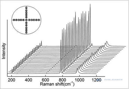
The data has three indicators: the position of the peak, the height of the peak (light intensity), and the width of the peak. Only when the peak position is completely matched, can it be o 4H-SiC qualificado. Assim como no DRX, sempre que houver outros picos, são substâncias de outras fases, o que é um defeito.
The difference in the position of the peak is due to the difference in the energy of the phonons brought about by the different silicon carbide crystal lattices, that is, the different frequencies. Each phonon has its corresponding energy level. The virtual energy level theory can be used to explain Raman (non-linear process):
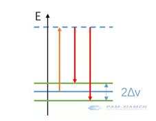
A partícula absorve a luz incidente até o nível de energia virtual (laranja) e, em seguida, faz a transição de volta para um nível de energia vibracional (vermelho) diferente do nível de energia original. Como o nível de energia superior é um nível de energia virtual, a frequência da luz incidente pode ser variada, desde que não entre em conflito com o nível de energia real original.
É importante notar que o modo LOPC (964,769 cm-1) pode ser usado para analisar a concentração do portador:
n = 1.25 * 1017cm-2 *(964.769cm-1-VLOPC measurement)
As the carrier concentration increases, the interaction between atoms and the lattice increases, which makes the Raman peak blue shift (smaller), the intensity decreases, and the width increases. This method is not as accurate as other methods and can only be used as an aid to analyze the silicon carbide crystal distribution.
3. Why not Use XRD to Measure Silicon Carbide Crystal Distribution?
X-rays are optical radiation generated by the transition of electrons in the inner layer of atoms under the bombardment of high-speed moving electrons, including continuous X-rays and characteristic X-rays. Silicon carbide single crystal can be used as X-ray gratings, and the coherent scattering produced by these large numbers of particles (atoms, ions, or molecules) will cause light interference, increasing or decreasing the intensity of scattered X-rays. Due to the superposition of scattered waves from a large number of particles, the beams that interfere with each other to produce the highest intensity are called X-ray diffraction lines.
Para atender às condições de difração, a fórmula de Bragg pode ser aplicada: 2dsinθ = nλ.
O feixe incidente faz com que cada dispersor re-irradie uma pequena parte de sua intensidade como uma onda esférica. Se os dispersores estiverem dispostos simetricamente com o intervalo d, essas ondas esféricas serão sincronizadas apenas na direção em que sua diferença de comprimento de caminho 2dsinθ é igual a um múltiplo inteiro do comprimento de onda λ. Nesse caso, uma parte do feixe incidente é desviada por um ângulo de 2θ, o que produzirá pontos de reflexão no padrão de difração.
Use X-rays of known wavelengths to measure the θ angle to calculate the interplanar spacing d, which is used for X-ray structure analysis; the other is to use a silicon carbide seed crystal with a known d to measure the θ angle to calculate the characteristic X-ray wavelength, and then the elements contained in the sample can be found in the existing data.
The measurement formula is 2dSinθ=λ. While the d value among the cubic silicon carbide crystal is close, and the characteristic is not obvious enough, the accurate silicon carbide crystal distribution cannot be precisely determined. For these reasons, it is not suitable to use the XRD to measure the distribution of silicon carbide crystals.

Para obter mais informações, entre em contato conosco pelo e-mail victorchan@powerwaywafer.com e powerwaymaterial@gmail.com.