We are an expert of semiconductor wafers in semiconductor industry, and we offer technology support and wafers selling for thousands of univerisities and industrial customers by our decades experience, including Cornell University, Stanford Univeristy,Peking University, Shandong Univerity, university of south carolina,Caltech Faraon lab (USA),University of California, Irvine (USA),Singapore MIT Alliance for Research and Technology Centre (SMART),West Virginia University,Purdue Univerity, University of California, Los Angeles,King Abdullah University of Science & Technology,Massachusetts Institute of Technology,University of Houston,University of Wisconsin,University of Science and Technology of China etc.
And now we show one article example as follows, who bought our wafers or service:
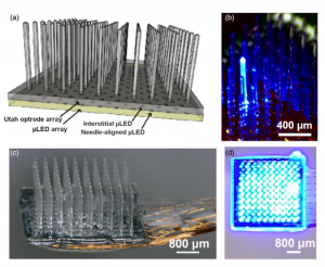
Article title:Multisite microLED optrode array for neural interfacing
Published by:
Niall McAlinden; Yunzhou Cheng; Robert Scharf; Enyuan Xie; Erdan Gu; Christopher F. Reiche; Rohit Sharma; Prashant Tathireddy; Prashant Tathireddy; Loren Rieth; Steve Blair; Keith Mathieson
1.Univ. of Strathclyde (United Kingdom)
2.The Univ. of Utah (United States)
3.The Univ. of Utah (United Kingdom)
4.The Feinstein Institute for Medical Research (United States)
Picture of LED wafer:
Abstract
We present an electrically addressable optrode array capable of delivering light to 181 sites in the brain, each providing sufficient light to optogenetically excite thousands of neurons in vivo, developed with the aim to allow behavioral studies in large mammals. The device is a glass microneedle array directly integrated with a custom fabricated microLED device, which delivers light to 100 needle tips and 81 interstitial surface sites, giving two-level optogenetic excitation of neurons in vivo. Light delivery and thermal properties are evaluated, with the device capable of peak irradiances >80 mW / mm2 per needle site. The device consists of an array of 181 80 μm × 80 μm2 microLEDs, fabricated on a 150-μm-thick GaN-on-sapphire wafer, coupled to a glass needle array on a 150-μm thick backplane. A pinhole layer is patterned on the sapphire side of the microLED array to reduce stray light. Future designs are explored through optical and thermal modeling and benchmarked against the current device.
Article abstract for Using Wafer from Xiamen Powerway Advanced Material Co. Ltd. (PAM-XIAMEN) or Powerway Wafer Co.,Limited
“… The microLED array is fabricated from 3-in. GaN-on-sapphire wafers (Xiamen Powerway Advanced Material) with a 400 – μ m -thick sapphire substrate and a 5 – μ m epitaxial GaN layer stack. 34 Full fabrication details are included in Fig …”
Source:
https://www.spiedigitallibrary.org/journals/Neurophotonics/volume-6/issue-3/035010/Multisite-microLED-optrode-array-for-neural-interfacing/10.1117/1.NPh.6.3.035010.full?SSO
About Xiamen Powerway Advanced Material Co., Ltd
Found in 1990,Xiamen Powerway Advanced Material Co., Ltd (PAM-XIAMEN) is a leading manufacturer of compound semiconductor material in China. PAM-XIAMEN develops advanced crystal growth and epitaxy technologies, manufacturing processes, engineered substrates and semiconductor devices. PAM-XIAMEN’s technologies enable higher performance and lower cost manufacturing of semiconductor wafer.
Now PAM-XIAMEN offer GaN material including GaN substrate, GaN on sapphire, InGaN, InN, and AlN epitaxial wafer with a wide range of deposition rates, various doping levels, wide composition ranges, and low defect densities. As well as GaN based LED wafer and AlGaN/GaN HEMT wafer.
PAM-XIAMEN also offer SiC and GaAs/InP material from wafer substrate to epitaxial growth.
Powerway Wafer Co.,Limited is a sub company of Xiamen Powerway Advanced Material Co., Ltd specialize in dealing with overseas orders.
Are You Looking for an Semiconductor wafer?
PAM-XIAMEN is proud to offer semiconductor wafer inlcuidng SiC/GaN/GaAs/InP wafer with wafer or epitaxial wafer for all different kinds of projects. If you are looking for semiconductor wafer, send us enquiry today to learn more about how we can work with you to get you the substrate wafers you need for your next project. Our group team is looking forward to providing both quality products and excellent service for you! For more information, please visit our website:www.powerwaywafer.com, send us email at tech@powerwaywafer.com or powerwaymaterial@gmail.com.