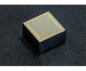
PAM-XIAMEN oferece substrato gálio nitreto bolacha para UHB-LED, gálio nitreto de bolacha, LD e outros dispositivos semicondutores.

SiC Wafer
Silicon Carbideï¼SiC) Wafers PAM-XIAMENÂ oferece carboneto de silício wafers crytal e epitaxia, que é usado para optoeletrônicos Devices, alta dispositivos de energia, dispositivos de alta temperatura, alta freqüência dispositivos de energia
GaAs Wafer
PAM-XIAMEN oferece substrato gálio arsenieto de bolacha e epitaxia para LED, LD e aplicações Microelectronics

germânio Wafer
PWAMÂ oferece materiais semicondutores, (Ge) monocristais germânio e bolachas cultivadas por VGF / LEC
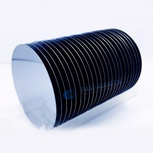
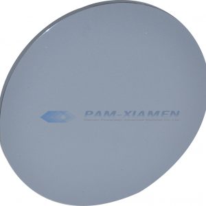
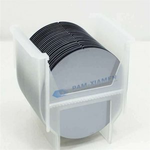
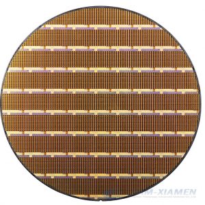
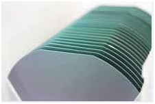
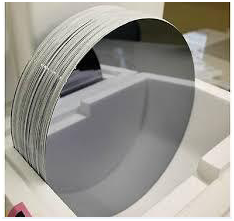
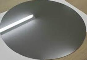
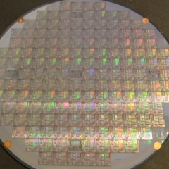
Silicon Wafer
PAM-XIAMEN, uma empresa de fabricação de wafer de silício, oferece wafer de silício: FZ Silicon wafer, Test Wafer Monitor Wafer Manequim Wafer, Test Wafer, CZ wafer, wafer epitaxial, wafer polido, wafer de gravação.
O processo de fabricação de wafer de silício é extração de cristal, corte de wafer de silício, moagem de wafer de silício, chanframento, gravação, polimento, limpeza e inspeção, entre os quais extração de cristal, polimento e inspeção de wafer de silício são os principais elos da fabricação de wafer de silício. Como substrato semicondutor básico, os wafers de silício devem ter altos padrões de pureza, planicidade da superfície, limpeza e contaminação de impurezas para manter as funções originais do chip. Os requisitos de alta especificação dos wafers de silício semicondutores tornam seu processo de fabricação complicado. As quatro etapas principais incluem purificação de polissilício e fundição de lingotes de polissilício, crescimento de wafer de silício de cristal único e corte e modelagem de wafer de silício. Como matéria-prima para a fabricação de wafers, a qualidade dos wafers de silício determina diretamente a estabilidade do processo de aplicação do wafer de silício. As pastilhas de silício de tamanho grande tornaram-se a tendência de desenvolvimento futuro das pastilhas de silício. A fim de melhorar a eficiência da produção e reduzir os custos, são usados cada vez mais pastilhas de silício de grande porte.

de fabricação de wafer
PAM-XIAMEN Oferece placa fotorresistente com fotorresistente e fotomáscara, e fornecer Nanolithography (fotolitografia): Preparação da superfície, Photoresist aplicar, coza macio, alinhamento, de exposição, de desenvolvimento, duro assar, Develop inspeccionar, Etch, remoção Photoresist (tira), controlo final.
-
12 "Prime Grade Silicon Wafer
A PAM-XIAMEN oferece wafers de silício nu de 300 mm (12 polegadas) em grau nobre, tipo n ou tipo p, e a espessura do wafer de silício de 300 mm é 775±15. Comparado com outros fornecedores de wafer de silício, o preço do wafer de silício da Powerway Wafer é mais competitivo com maior qualidade. Os wafers de silício de 300 mm têm um rendimento maior por wafer do que os wafers de silício de grande diâmetro permeáveis.
-
12 "wafers de silício 300 milímetros TOX (Si térmica Oxidação Wafer)
PAM-XIAMEN oferece wafer de óxido de silício de 300 mm e wafer de dióxido. A bolacha de silício de óxido térmico ou bolacha de dióxido de silício é uma bolacha de silício nua com camada de óxido cultivada por processo de oxidação seco ou úmido. A camada de óxido térmico do wafer de silício é geralmente cultivada em um forno de tubo horizontal, e a faixa de temperatura do óxido de wafer de silício é geralmente de 900 ℃ ~ 1200 ℃. Comparado com a camada de óxido CVD, a camada de óxido de wafer de silício tem maior uniformidade, melhor compacidade, maior rigidez dielétrica e melhor qualidade.
-
12 "Test Grade Silicon Wafer
O PAM-XIAMEN oferece wafers de silício nu de 300 mm (12 polegadas) fictício, grau de teste, tipo n ou tipo p. Em comparação com outros fornecedores de pastilhas de silício, a Powerway Wafer oferece serviços profissionais com preços competitivos.
-
Epi bolacha por Laser Diode
O wafer de epitaxia LD baseado em GaAs, que pode gerar emissão de estímulo, é amplamente utilizado para fabricar diodo laser, uma vez que as propriedades superiores do wafer epitaxial de GaAs tornam o dispositivo um baixo consumo de energia, alta eficiência, longa vida útil e etc. , os materiais semicondutores comumente usados são sulfeto de cádmio (CdS), fosfeto de índio (InP) e sulfeto de zinco (ZnS).
-
Flutuar-Zone Mono-Crystalline Silicon
A PAM-XIAMEN pode oferecer wafer de silício de zona flutuante, que é obtido pelo método Float Zone. As hastes de silício monocristalino são obtidas através do crescimento da zona flutuante e, em seguida, processam as hastes de silício monocristalino em pastilhas de silício, chamadas pastilhas de silício da zona flutuante. Uma vez que a pastilha de silício fundida por zona não está em contato com o cadinho de quartzo durante o processo de silício por zona flutuante, o material de silício está em estado suspenso. Assim, é menos poluído durante o processo de fusão da zona flutuante de silício. O teor de carbono e o teor de oxigênio são menores, as impurezas são menores e a resistividade é maior. É adequado para a fabricação de dispositivos de energia e certos dispositivos eletrônicos de alta tensão.
-
Serviços de fundição de wafer
A PAM-XIAMEN fornece serviços de fundição de wafer com tecnologia avançada de processo de semicondutores e se beneficia de nossas experiências upstream de substrato e wafer expaxy,
PAM-XIAMEN deve ser a mais avançada tecnologia de wafer e serviços de fundição para empresas sem fábulas, IDMs e pesquisadores.
-
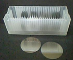
Teste Wafer Monitor de bolacha manequim Wafer
Como fabricante de wafer fictício, a PAM-XIAMEN oferece wafer fictício de silicone / wafer de teste / wafer monitor, que é usado em um dispositivo de produção para melhorar a segurança no início do processo de produção e é usado para verificação de entrega e avaliação da forma do processo. Como as pastilhas de silício fictícias são frequentemente usadas para experimentos e testes, o tamanho e a espessura das mesmas são fatores importantes na maioria das ocasiões. wafer fictício de 100 mm, 150 mm, 200 mm ou 300 mm está disponível.
-
Cz Mono-Crystalline Silicon
PAM-XIAMEN, um produtor de silício monocristalino a granel, pode oferecer wafers de silício monocristalino <100>, <110> e <111> com dopante N&P em 76,2~200 mm, que são cultivados pelo método CZ. O método de Czochralski é um método de crescimento de cristais, conhecido como método CZ. Ele é integrado em um sistema de calor de tubo reto, aquecido por resistência de grafite, derrete o polissilício contido em um cadinho de quartzo de alta pureza e, em seguida, insere o cristal de semente na superfície do fundido para soldagem. Depois disso, o cristal de semente rotativo é abaixado e derretido. O corpo é infiltrado e tocado, gradualmente levantado e finalizado ou puxado através das etapas de pescoço, pescoço, ombro, controle de diâmetro igual e acabamento.
-
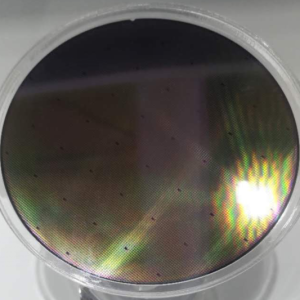
Epitaxial Silicon Wafer
A bolacha epitaxial de silício (epi wafer) é uma camada de cristal único de silício epitaxial depositado em uma bolacha de silício de cristal único (nota: está disponível para crescer uma camada de camada de silício policristalino em cima de uma bolacha de silício monocristalino altamente dopada, mas precisa de camada de buffer (como óxido ou poli-Si) entre o substrato de Si a granel e a camada de silício epitaxial superior.Também pode ser usado para transistor de filme fino.
-
Wafer polido
PAM-XIAMEN pode oferecer wafer polido, tipo n ou tipo p com orientação em <100>, <110> ou <111>. Wafers polidos FZ, principalmente para a produção de retificador de silício (SR), retificador controlado de silício (SCR), transistor gigante (GTR), tiristor (GRO)
-
gravura Wafer
As pastilhas de silício de gravação oferecidas pela PAM-XIAMEN são pastilhas de gravação do tipo N ou P, que possuem baixa rugosidade, baixa refletividade e alta refletividade. O wafer de gravação tem as características de baixa rugosidade, bom brilho e custo relativamente baixo, e substitui diretamente o wafer polido ou wafer epitaxial que tem custo relativamente alto para produzir os elementos eletrônicos em alguns campos, reduzindo os custos.
-
Fotoresiste de nanofabricação
PAM-XIAMEN Oferece placa fotorresistente com fotorresistente