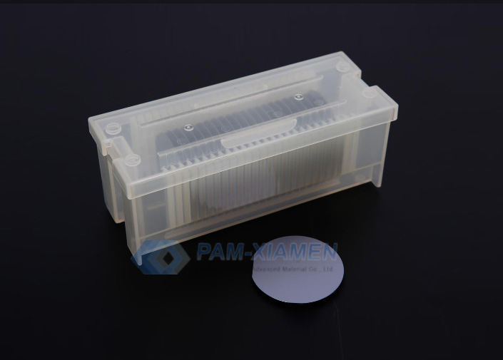
Dia 3 inch semi insulating GaAs substrate is available. GaAs materials are mainly divided into two categories: semi-insulating gallium arsenide material and semiconductor gallium arsenide material. Here we will discuss the semi-insulating gallium arsenide material. Semi-insulating property is a basic physical property of gallium arsenide material, and it is a very important property. Through regional ion implantation, the inside of the semi-insulating gallium arsenide substrate an still maintain electrical isolation. So the semi-insulating GaAs substrate is very suitable for the production of integrated circuits. In addition, the parasitic capacitance of the device made of semi-insulating gallium arsenide substrate is very small, which can be used to manufacture some fast devices, such as monolithic microwave integrated circuits. please see below specification:
1. Specification of Semi Insulating GaAs Substrate 3 Inch
| Parâmetros | Especificações |
| Material | VGF GaAs único cristal Wafer |
| Grau | Prime, Epi-Ready |
| doping | Semi-Insulating, C doped |
| wafer OD | 76,2 +/- 0,63 milímetros |
| wafer Orientação | (100) +/- 0,25 ° C. |
| Comprimento Plano primária | 22,22 +/- 3,17 milímetros |
| Comprimento Plano secundário | 11,15 +/- 1,52 milímetros |
| Primária Plano Local | (01-1) +/- 0.5◦ deg. (SEMI EUA) |
| Plano secundário Location |
(011) +/- 0,5 graus. (SEMI EUA) |
| Plano Primário / Secundário Orientation |
90◦ +/- 0.5◦ |
| Plano secundário é perpendicular à Primária Apartamento em Contador sentido horário | |
| Concentração transportadora | <1E8 / cc |
| Resistividade | > 1E7Ohm-cm |
| Mobilidade | > 6000 cm2 / V-sec |
| EPD | <5000 / cm2 |
| Espessura | 625 +/- 25 pm |
| TTV | </ = 8.00μm |
| Arco | </ = 10.00μm |
| Acabamento de superfície | Lado 1: polido Side 2 : Etched |
| Laser Mark | Na parte da frente, perto bemol maior (Vendor to provide Wafer identification Number on the Wafer near the Major Flat) |
| Qualidade | Arranhões, chips de Borda, Sawmarks, Cracks, Pits, Haze & Orange peel should not be present. |
| SEMI-padrão | M 9,2-89 |
2. Application and Significance of Semi-insulating GaAs Substrate
Gallium arsenide materials are mainly divided into two categories: semi-insulating gallium arsenide materials and semiconductor gallium arsenide materials. Semi insulating gallium arsenide materials are mainly used to produce integrated circuits with MESFET, HEMT and HBT structures, and mainly used in radar, microwave and millimeter wave communications, ultra-high-speed computers and optical fiber communications.
In the field of microelectronics, semi-insulating GaAs is used as the substrate. Due to the characteristics of high electron mobility, large band gap, direct band gap, and low power consumption, semi-insulating substrates are used to make high-speed digital circuits, microwave monolithic circuits, optoelectronics, and integrated circuits and high-power field effect transistors, which have the characteristics of fast speed, high frequency, low power consumption and radiation resistance. Semi insulating substrate is not only of great significance in national defense, but also widely used in civil and national economic construction. In the communication field, semi-insulating gallium arsenide materials are mainly used in high-frequency communication devices. In recent years, driven by the civilian wireless communication market, especially the mobile phone market, the semi insulating GaAs substrate market scale has also grown rapidly. In the process of commercialization of 5G, it plays an irreplaceable role.

Para mais informações, entre em contato conosco pelo e-mailvictorchan@powerwaywafer.com e powerwaymaterial@gmail.com.