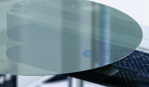
Silicon carbide (SiC) wafer material supplied by PAM-XIAMEN, like SiC substrate (link: https://www.powerwaywafer.com/sic-wafer/sic-wafer-substrate.html) is widely used in aerospace, radar communication, automotive industry and semiconductor industry due to its excellent properties such as high thermal conductivity, high strength, high temperature resistance and radiation resistance. However, during the preparation, processing and use of SiC single crystal materials, certain residual stress will be generated due to the existence of defects such as micropipes, dislocations, small-angle boundaries and inclusions. For SiC single crystal materials, the formation of residual stress is the superposition of thermal stress, stress due to defects and machining stress. So, residual stress is often used as an important indicator to measure the quality of components. Usually inappropriate residual stress will damage the integrity of SiC single crystal material, resulting in unnecessary deformation and failure of components. Therefore, it is necessary to detect the residual stress of silicon carbide single crystal materials. We recommend you some methods for detecting residual stress of SiC single crystal.
At present, the measurement methods of residual stress of single crystal materials mainly include photoelastic method, X-ray diffraction method, micro-Raman spectroscopy, neutron diffraction method and so on. Among them, photoelastic method and X-ray diffraction method are widely used in stress detection of single crystal materials. More specifically as follows:
1. Photoelastic Method
Photoelasticity is an experimental method that uses optical principles to study the stress distribution of materials. Brewster first discovered the phenomenon of photoelasticity. Then Max-well linked birefringence with stress and established the optical law of stress, which accelerated the development of photoelasticity.
The photoelastic method for detecting residual stress in single crystal materials is based on the birefringence characteristics of optical crystal materials, that is, two different refractive indices are produced when a beam of light passes through a certain material. The stress detection principle of this method is as follows: As shown in Figure 1, when a beam of light passes through a photoelastic material, it will be decomposed into two beams with different propagation velocities along the two principal stresses σ 1 and σ 2 directions due to the existence of stress. The plane polarized light of , thus generating a relative optical path difference, the principal stress of the material can be determined according to the optical law of stress shown in formula (1), and then the light is transmitted through the analyzer to produce light interference, and the stress of the component is obtained. The photoelastic fringe image of the information, from which the stress state and distribution in the component can be deduced:
In the formula: m is a positive integer related to the optical fringe series; λ is the wavelength of the light source; C1-C2 is the stress optical constant; f=λ/(C1-C2) is the fringe value of the photoelastic material; h is the model thickness.
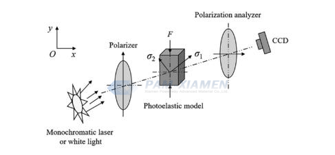
Fig.1 Principle Schematic of Photoelastic Method
The photoelastic method has the advantages of real-time, non-contact, non-destructive and global, and can detect the stress of complex two-dimensional and three-dimensional spatial structures. Therefore, this method has been widely studied and applied in the stress detection of single crystal materials.
2. X-Ray Diffraction
X-ray diffraction is a non-destructive testing method for testing residual stress on the surface of single crystal materials. X-ray diffraction method is based on elastic mechanics theory and X-ray diffraction theory to realize stress detection of materials. The basic principle is that when there is residual stress in the component, the spacing between the crystal planes in the grain will change regularly with the magnitude of the stress. The strain value of the material is obtained by measuring the change of the interplanar spacing by X-ray diffraction, and then the residual stress value of the member is calculated according to Hooke’s law and using an appropriate stiffness relationship. At present, the methods mainly include Imura method, Ortner method and multiple linear regression method.
3. Micro Raman Spectroscopy
Micro-Raman spectroscopy is an emerging and promising micro-scale experimental mechanical testing technology. Using this technique to detect residual stress in single crystal materials is based on the principle of Raman scattering. The basic principle is that when there is residual stress in the material, the Raman frequency shift will change with the lattice deformation. By detecting changes in Raman spectral lines, using the relationship between the stress and the relative Raman frequency shift shown in formula (2), the stress of the single crystal material can be obtained

In fomula (2): Ψ is the stress/strain-frequency shift factor of the material; Δω is the frequency shift increment
With the advantages of non-contact, non-destructive, real-time, high sensitivity and high spatial resolution, micro-Raman spectroscopy has been widely used in micro-scale experimental mechanics, especially in the field of mechanical measurement of semiconductor materials.
4. Neutron Diffraction
The neutron diffraction method is a detection and analysis method that can directly obtain the three-dimensional stress distribution inside the component without damage to the component. It is based on Bragg’s law to realize the determination of residual stress of single crystal materials. The basic principle of the method is as follows: the distance between the lattices in the unit cell is measured by the neutron diffractometer, the elastic strain is solved by the change of the distance, and then the stress distribution of the component is obtained according to the relationship between the strain and the stress. The neutron diffraction method has the advantages of large penetration depth and high spatial resolution.
Fig. 2 Schematic Diagram of Residual Stress Measurement by Neutron Diffraction Method
Here is a comparison of different residual stress detection methods for your reference as figure 3:
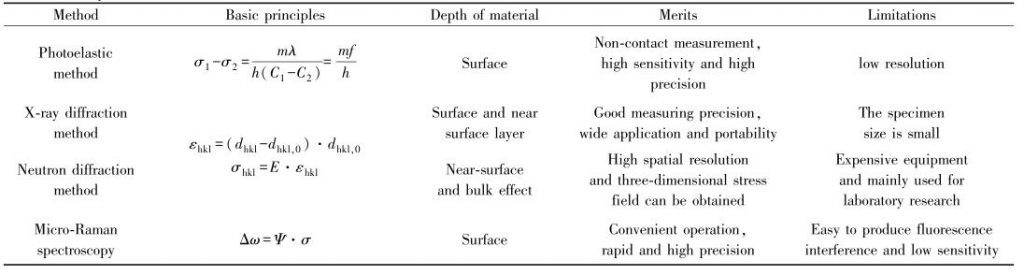
Fig. 3 Comparison of Stress Detection Methods

For more information, please contact us email at victorchan@powerwaywafer.com and powerwaymaterial@gmail.com.