GaN HEMT Эпитаксиальная пластина
Gallium Nitride (GaN) HEMTs (High Electron Mobility Transistors) are the next generation of RF power transistor technology. Thanks to GaN technology, PAM-XIAMEN now offer AlGaN/GaN HEMT Epi Wafer on sapphire or Silicon, and AlGaN/GaN on sapphire template.
- Описание
Описание продукта
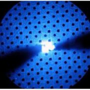
GaN HEMT epitaxial wafer is a multilayer film grown epitaxially on a substrate, which usually includes a nucleation layer, a transition layer, a buffer layer, a channel layer, a barrier layer, a cap layer, and a passivation layer from bottom to top. The nucleation layer, like AlGaN or AlN, is used to prevent the substrate material from diffusing into the GaN epitaxial layer. The transition layer may contain hierarchical AlGaN, AlN/GaN superlattice or multilayer AlN to balance the stress between the GaN and the substrate. The higher the Al content in the barrier layer of AlGaN, the higher the 2DEG concentration at the heterojunction. Meanwhile, the lower the threshold voltage of the device, and the higher the current capacity. As the Al ratio increasing, the degree of heterogeneous crystal lattice mismatch will be higher, resulting in a decrease in gallium nitride HEMT electron mobility and a decrease in current capacity.
The High Electron Mobility Transistor (HEMT) is developed based on GaN with unique heterostructure and two-dimensional electron gas. The GaN HEMT advantages include high breakdown strength, low on-resistance and faster The switching speed, which is very suitable for medium and low voltage and medium and small power systems, such as travel adapters, wireless chargers, AC-DC converters, smart home appliances, etc. The epitaxial wafer with HEMT structure is more attractive currently for high-frequency converters, in which GaN HEMT breakdown voltage is 600~650 V. With the rapid development of gallium nitride HEMT epi technology, the price of GaN HEMT devices will be competitive, which can gain large GaN HEMT market for GaN HEMT manufacturers. Moreover, due to the gallium nitride HEMT reliability, it can be widely used in industrial fields, such as photovoltaic inverters, energy storage systems, and electric vehicles.
1. GaN HEMT Material: Available size:2”,4”,6”,8”:
More specific parameters of gallium nitride HEMT wafer for D-mode GaN HEMTs, E-mode GaN HEMTs, GaN HEMT power amplifier and RF, please refer to:
GaN на Si для питания, D-режиме
We are expert in HEMT structure, we also offer GaN HEMT epi wafer for many years.
For silicon substrate, we need to know if you grow GaN HEMT on silicon for POWER or RF, it is different. If needed, please contact victorchan@powerwaywafer.com for details.
For SiC, you should use semi-insulating.
Or you can buy AlGaN/GaN HEMT structure on these three structure from us.
2. Now we show you an example as follows:
2.1 2 ″ (50,8 мм) эпитаксиальные вафли GaN HEMT
We offer 2″(50.8mm) gallium nitride HEMT Wafers, the GaN HEMT structure is as follows:
Структура (сверху вниз):
* Нелегированный GaN колпачок (2 ~ 3nm)
AlxGa1-х ^ (18 ~ 40 нм)
AlN (буферный слой)
ун-легированных GaN (2 ~ 3 мкм)
сапфировой подложки
* Мы можем использовать Si3N для замены GaN сверху, адгезия сильная, он покрыт напылением или PECVD.
2.2 AlGaN/GaN HEMT Epi Wafer on sapphire/GaN
| слой # | Состав | Толщина | X | добавка | Концентрация носителей |
| 5 | GaN | 2нм | – | – | – |
| 4 | AlxGa1-х ^ | 8 нМ | 0.26 | – | – |
| 3 | AlN | 1nm | Un-легированный | ||
| 2 | GaN | ≥1000 нм | Un-легированный | ||
| 1 | Буфер / переходный слой | – | – | ||
| подложка | кремний | 350μm / 625μm | – | ||
2.3 2″(50.8mm),4″ (100mm)AlGaN/GaN HEMT Epi Wafer on Si
2.3.1 Specifications for Aluminium Gallium Nitride (AlGaN) / Gallium Nitride (GaN) Транзистор с высокой подвижностью электронов (HEMT) на кремниевой подложке.
| Требования | Спецификация |
| AlGaN / GaN HEMT Эпи вафли на Si | |
| Структура НЕМТ / GaN, AlGaN | См 1.2 |
| Материал подложки | кремний |
| Ориентация | <111> |
| метод роста | Поплавок зоны |
| Проводимость Тип | P или N |
| Размер (дюйм) | 2” , 4” |
| Толщина (мкм) | 625 |
| задница | Грубый |
| Удельное сопротивление (Ω см) | >6000 |
| Лук (мкм) | ≤ ± 35 |
2.3.2 Epi structure: Crack-free Epilayers
| слой # | Состав | Толщина | X | добавка | Концентрация носителей |
| 5 | GaN | 2нм | – | – | – |
| 4 | AlxGa1-х ^ | 8 нМ | 0.26 | – | – |
| 3 | AlN | 1nm | Un-легированный | ||
| 2 | GaN | ≥1000 нм | Un-легированный | ||
| 1 | Буфер / переходный слой | – | – | ||
| подложка | кремний | 350μm / 625μm | – | ||
2.3.3 Electrical Properties of the AlGaN/GaN HEMT structure
2DEG Mobility (при 300 К): ≥1800 см2 / В
2DEG Плотность несущей (при 300 К): ≥0,9 × 10¹³ см-2
Среднеквадратичная шероховатость (AFM): ≤ 0,5 нм (площадь сканирования 5,0 мкм × 5,0 мкм)
2.4 2″(50.8mm)AlGaN/GaN on sapphire
Для спецификации AlGaN / GaN на сапфировом шаблоне, пожалуйста, свяжитесь с нашим отделом продаж: sales@powerwaywafer.com.
GaN HEMT Applications: Used in blue laser diodes, ultraviolet LEDs (down to 250 nm), and AlGaN/GaN HEMTs device.
3. Explanation of AlGaN/Al/GaN HEMTs:
Нитридные HEMT интенсивно разрабатываются для мощной электроники в приложениях высокочастотного усиления и коммутации мощности. Часто высокая производительность в режиме постоянного тока теряется при переключении HEMT - например, при отключенном токе происходит сбой при импульсном сигнале затвора. Считается, что такие эффекты связаны с захватом заряда, который маскирует влияние затвора на протекание тока. Полевые пластины на электродах источника и затвора использовались для управления электрическим полем в устройстве, смягчая такие явления коллапса тока.
4. GaN EpitaxialTechnology — Customized GaN epitaxy on SiC,Si and Sapphire substrate for HEMTs, LEDs:
GAN HEMT EPITAXIAL WAFERS (GAN EPI-WAFERS)
PAM XIAMEN Offers Epitaxial growth of AlGaN/GaN based HEMT on Si wafers
5. GaN Device:
GaN HEMT
6. Test Characterization Equipment:
Бесконтактный Сопротивление листа
Лазерная картография толщины тонкой пленки
Высокотемпературный / высокая влажность обратного смещения
Тепловой удар
DIC Nomarski микроскоп
Атомно-силовой микроскоп (АСМ)
Поверхностные Defectivity Scan
Высокий темп обратного смещения
4ППЫ Сопротивление листа
Бесконтактный Hall Mobility
Температура цикла
Дифракция рентгеновских лучей (XRD) / Отражение (XRR)
эллипсометре Толщина
профилометр
CV Tester
7. Foundry Fabrication:
we also offer foundry GaN HEMT fabrication in the following process as follows:
МОС-гидридной эпитаксии
Металл Распыление / E-Beam
Dry / Wet металл / диэлектрик Etch
Тонкая пленка PECVD / LPCVD / Распыление
RTA / печи Отжиг
Фотолитография (0,35 мкм мин. CD)
ионная имплантация
Remark:
The Chinese government has announced new limits on the exportation of Gallium materials (such as GaAs, GaN, Ga2O3, GaP, InGaAs, and GaSb) and Germanium materials used to make semiconductor chips. Starting from August 1, 2023, exporting these materials is only allowed if we obtains a license from the Chinese Ministry of Commerce. Hope for your understanding and cooperation!
More fabrication services, please visit: GaN Fabrication Services for HEMT Devices
Алюминий-галлиевый арсенид эпи-вафель
650V GaN FETs Chip for Fast Charge
GaN MOSFET Structure:
GaN MOSFET Structure on SiC Substrate
More about GaN HEMT structures, please read:
Вам также может понравиться ...
-
SiC вафельного Субстрат
Компания имеет полную линию по производству подложек для пластин SiC (карбида кремния), объединяющую выращивание кристаллов, обработку кристаллов, обработку пластин, полировку, очистку и тестирование. В настоящее время мы поставляем коммерческие пластины SiC 4H и 6H с полуизоляцией и проводимостью как на оси, так и вне оси, доступные размеры: 5x5 мм2, 10x10 мм2, 2", 3", 4", 6" и 8", прорывая ключевые технологии, такие как такие как подавление дефектов, обработка затравочных кристаллов и быстрый рост, содействие фундаментальным исследованиям и разработкам, связанным с эпитаксией карбида кремния, устройствами и т. д.
-
на основе GaN LED эпитаксиальные вафельные
GaN-PAM-СЯМЫНЬ (в нитрида галлия) основе LED эпитаксиальных пластин для ультра высокой яркости синего и зеленого светоизлучающих диодов (LED) и лазерных диодов (LD) приложений.
-
Ge (германий) монокристаллы и Вафли
PAM-XIAMEN предлагает германиевые пластины размером 2”, 3”, 4” и 6”, что является сокращением от Ge-подложки, выращенной VGF/LEC. Слегка легированная германиевая пластина типа P и N также может быть использована для эксперимента по эффекту Холла. При комнатной температуре кристаллический германий хрупкий и малопластичный. Германий обладает полупроводниковыми свойствами. Германий высокой чистоты легируют трехвалентными элементами (такими как индий, галлий, бор) для получения германиевых полупроводников P-типа; а пятивалентные элементы (такие как сурьма, мышьяк и фосфор) легируются для получения германиевых полупроводников N-типа. Германий обладает хорошими полупроводниковыми свойствами, такими как высокая подвижность электронов и высокая подвижность дырок. -
GaSb вафельные
PAM-XIAMEN offers Compound Semiconductor GaSb wafer – gallium antimonide which are grown by LEC(Liquid Encapsulated Czochralski) as epi-ready or mechanical grade with n type, p type or semi-insulating in different orientation(111) or (100).
-
GaN шаблоны
Шаблонные продукты PAM-XIAMEN состоят из кристаллических слоев шаблонов GaN (нитрида галлия), AlN шаблона (нитрида алюминия), AlGaN шаблонов (нитрида галлия алюминия) и шаблонов InGaN (нитрида индия-галлия), которые наносятся на сапфир -
Float-Zone монокристаллического кремния
PAM-XIAMEN может предложить кремниевую пластину с зоной плавания, полученную методом зоны плавания. Монокристаллические кремниевые стержни получают путем выращивания в зоне плавания, а затем перерабатывают монокристаллические кремниевые стержни в кремниевые пластины, называемые кремниевыми пластинами с плавающей зоной. Поскольку кремниевая пластина зонной плавки не контактирует с кварцевым тиглем во время процесса кремния с плавающей зоной, кремниевый материал находится во взвешенном состоянии. Тем самым он меньше загрязняется в процессе зонной плавки кремния. Содержание углерода и кислорода ниже, примесей меньше, удельное сопротивление выше. Он подходит для производства силовых устройств и некоторых высоковольтных электронных устройств.
-
GaAs Epiwafer
PAM-XIAMEN is manufacturing various types of epi wafer III-V silicon doped n-type semiconductor materials based on Ga, Al, In, As and P grown by MBE or MOCVD. We supply custom GaAs epiwafer structures to meet customer specifications, please contact us for more information.
-
Корпусная GaN-подложка
РАМ-СЯМЫНЬ установила технологии изготовления для автономных (нитрид галлия) GaN-подложка пластины, которая является для UHB-LED и LD. Выращенный по технологии гидридной эпитаксии из паровой фазы (HVPE), Наша GaN-подложка имеет низкую плотность дефектов.


