


InAs вафельные
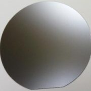
PAM-XIAMEN offers Compound Semiconductor InAs wafer – indium arsenide wafer which are grown by LEC(Liquid Encapsulated Czochralski) as epi-ready or mechanical grade with n type, p type or semi-insulating in different orientation(111) or (100). In addition, InAs single crystal has high electron mobility and is an ideal material for making Hall devices.
- Описание
Описание продукта
PAM-XIAMEN offers Compound Semiconductor InAs wafer – indium arsenide wafer which is grown by LEC(Liquid Encapsulated Czochralski) as epi-ready or mechanical grade with n type, p type or semi-insulating in different orientation(111)(100) or (110). In addition, InAs single crystal has high electron mobility and is an ideal material for making Hall devices.
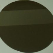
Indium arsenide, InAs, is a semiconductor composed of indium and arsenic. It has the appearance of grey cubic crystals with a melting point of 942 °C and lattice constant of 0.6058nm, and the indidum arsenide crystal structure is a zinc blende structure. Indium arsenide wafer is used for construction of infrared detectors, for the wavelength range of 1–3.8 µm. The detectors are usually photovoltaic photodiodes. Cryogenically cooled detectors have lower noise, but InAs detectors can be used in higher-power applications at room temperature as well. Because of the superior indium arsenide properties, indium arsenide thin films are also used for making of diode lasers.
Indium arsenide band gap is a direct transition, which is similar to gallium arsenide, and the forbidden band width is (300K)0.45eV. Indium arsenide is sometimes used together with indium phosphide. Alloyed with gallium arsenide, it forms indium gallium arsenide – a material with band gap dependent on In/Ga ratio, a method principally similar to alloying indium nitride with gallium nitride to yield indium gallium nitride.
Вот спецификация деталь:
2 "(50,8) Спецификация InAs вафли
3 "(76,2 мм) Спецификация InAs вафли
4 "(100 мм) Спецификация InAs вафли
2″ InAs Wafer Specification
| Item | Specifications | |||
| Dopant | low doped | Stannum | Sulphur | Zinc |
| Conduction Type | N-type | N-type | N-type | P-type |
| Wafer Diameter | 2″ | |||
| Wafer Orientation | (111)±0.5° , (110)±0.5° | |||
| Wafer Thickness | 500±25um | |||
| Primary Flat Length | 16±2mm | |||
| Secondary Flat Length | 8±1mm | |||
| Carrier Concentration | 5×1016cm-3 | (5-20)x1017cm-3 | (1-10)x1017cm-3 | (1-10)x1017cm-3 |
| Mobility | ≥2×104cm2/V.s | 7000-20000cm2/V.s | 6000-20000cm2/V.s | 100-400cm2/V.s |
| EPD | <5×104cm-2 | <5×104cm-2 | <3×104cm-2 | <3×104cm-2 |
| TTV | <10um | |||
| BOW | <10um | |||
| WARP | <12um | |||
| Laser marking | upon request | |||
| Suface finish | P/E, P/P | |||
| Epi ready | yes | |||
| Package | Single wafer container or cassette | |||
3″ InAs Wafer Specification
| Item | Specifications | |||
| Dopant | low doped | Stannum | Sulphur | Zinc |
| Conduction Type | N-type | N-type | N-type | P-type |
| Wafer Diameter | 3″ | |||
| Wafer Orientation | (111)±0.5° , (110)±0.5° | |||
| Wafer Thickness | 600±25um | |||
| Primary Flat Length | 22±2mm | |||
| Secondary Flat Length | 11±1mm | |||
| Carrier Concentration | 5×1016cm-3 | (5-20)x1017cm-3 | (1-10)x1017cm-3 | (1-10)x1017cm-3 |
| Mobility | ≥2×104cm2/V.s | 7000-20000cm2/V.s | 6000-20000cm2/V.s | 100-400cm2/V.s |
| EPD | <5×104cm-2 | <5×104cm-2 | <3×104cm-2 | <3×104cm-2 |
| TTV | <12um | |||
| BOW | <12um | |||
| WARP | <15um | |||
| Laser marking | upon request | |||
| Suface finish | P/E, P/P | |||
| Epi ready | yes | |||
| Package | Single wafer container or cassette | |||
4″ InAs Wafer Specification
| Item | Specifications | |||
| Dopant | low doped | Stannum | Sulphur | Zinc |
| Conduction Type | N-type | N-type | N-type | P-type |
| Wafer Diameter | 4″ | |||
| Wafer Orientation | (111)±0.5° , (110)±0.5° | |||
| Wafer Thickness | 900±25um | |||
| Primary Flat Length | 16±2mm | |||
| Secondary Flat Length | 8±1mm | |||
| Carrier Concentration | 5×1016cm-3 | (5-20)x1017cm-3 | (1-10)x1017cm-3 | (1-10)x1017cm-3 |
| Mobility | ≥2×104cm2/V.s | 7000-20000cm2/V.s | 6000-20000cm2/V.s | 100-400cm2/V.s |
| EPD | <5×104cm-2 | <5×104cm-2 | <3×104cm-2 | <3×104cm-2 |
| TTV | <15um | |||
| BOW | <15um | |||
| WARP | <20um | |||
| Laser marking | upon request | |||
| Suface finish | P/E, P/P | |||
| Epi ready | yes | |||
| Package | Single wafer container or cassette | |||
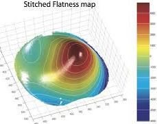
Stitched Flatness Map of InAs Wafer
Wafer Spec(example):
1) 2” (50,8 мм) InAs
Type/Dopant:N/S
Orientation:[111B]±0.5°
Thickness:500±25um
Epi-Ready
SSP
2) 2” (50,8 мм) InAs
Type/Dopant:N/low doped
Orientation : (111)B
Thickness:500um±25um
SSP
3) 2” (50,8 мм) InAs
Type/Dopant:N / low doped
Orientation : <111>A ±0.5°
Thickness:500um±25um
epi-ready
Ra<=0.5nm
Carrier Concentration(cm-3):1E16~3E16
Mobility(cm -2 ):>20000
EPD(cm -2 ):<15000
SSP
4) 2” (50,8 мм) InAs
Type/Dopant:N/low doped
Orientation : <100> with [001]O.F.
Thickness:2mm
AS cut
5) 2” (50,8 мм) InAs
Type/Dopant:N/P
Orientation :(100),
Carrier Concentration(cm-3):(5-10)E17,
Thickness:500 um
SSP
6)Indium Arsenide wafers,
2″Ø×500±25µm,
p-type InAs:Zn
(110)±0.5°,
Nc=(1-3)E18/cc ,
Both-sides-polished,
Sealed under nitrogen in single wafer cassette.
Все пластины предлагаются с высоким качеством эпитаксии готовой отделкой. Поверхности характеризуются в доме, передовые оптических методами, которые включают метрологический Surfscan мутность и мониторинг частиц, спектроскопическую эллипсометрию и скользящее падение интерферометрию
Влияние температуры отжига на оптические свойства поверхностных слоев накопления электронов в п-типа (1 0 0) InAs вафель была исследована с помощью спектроскопии комбинационного рассеяния. Он обладает, что комбинационное пики из-за рассеяния на неэкранированных фононов LO исчезают с повышением температуры, что свидетельствует о том, что накопление слоя электронов в поверхности InAs устраняется путем отжига. Участие механизм анализировали с помощью рентгеновской фотоэлектронной спектроскопии, рентгеновской дифракции и высокой разрешающей способностью просвечивающей электронной микроскопии. Результаты показывают, что аморфные In2O3 и As2O3 фаза образуются на поверхности InAs при отжиге и, тем временем, тонкая кристаллический, как слой на границе раздела между окисленным слоем и пластиной также генерируются, что приводит к уменьшению толщины накопления поверхностных электронного слой, поскольку, как адатомы ввести акцептор типа поверхностных состояний.
The emission wavelength of InAs is 3.34μm, and lattice-matched In-GaAsSb, InAsPSb and InAsSb multi-epitaxial materials can be grown on the indium arsenide substrates, which can manufacture lasers and detectors for optical fiber communication in the 2~4μm band.
We also offer InAs wafer epi service, take below as an example:
2”size InAs epi wafer(PAM190730-INAS):
Epi layer: Thikness 0.5 um, InAs epi layer(undoped, n type),
Substrate:2” semi-insulating GaAs
More details about InAs epi wafer, please refer to:
Относительные продукты:
InAs вафельные
InSb вафельные
InP пластины
GaAs вафельные
GaSb вафельные
GaP вафельные
Indium Arsenide Ingot with Zinc Blende Structure Grown By VGF
Вам также может понравиться ...
-
GaAs Epiwafer
PAM-XIAMEN is manufacturing various types of epi wafer III-V silicon doped n-type semiconductor materials based on Ga, Al, In, As and P grown by MBE or MOCVD. We supply custom GaAs epiwafer structures to meet customer specifications, please contact us for more information.
-
GaN HEMT эпитаксиальные вафельные
Gallium Nitride (GaN) HEMTs (High Electron Mobility Transistors) are the next generation of RF power transistor technology. Thanks to GaN technology, PAM-XIAMEN now offer AlGaN/GaN HEMT Epi Wafer on sapphire or Silicon, and AlGaN/GaN on sapphire template.
-
Подложка SiC вафли
Компания имеет полную линию по производству подложек для пластин SiC (карбида кремния), объединяющую выращивание кристаллов, обработку кристаллов, обработку пластин, полировку, очистку и тестирование. В настоящее время мы поставляем коммерческие пластины SiC 4H и 6H с полуизоляцией и проводимостью как на оси, так и вне оси, доступные размеры: 5x5 мм2, 10x10 мм2, 2", 3", 4", 6" и 8", прорывая ключевые технологии, такие как такие как подавление дефектов, обработка затравочных кристаллов и быстрый рост, содействие фундаментальным исследованиям и разработкам, связанным с эпитаксией карбида кремния, устройствами и т. д.
-
GaP Wafer – временно не предлагается
PAM-XIAMEN offers Compound Semiconductor GaP wafer – gallium phosphide wafer which is grown by LEC(Liquid Encapsulated Czochralski) as epi-ready or mechanical grade with n type, p type or semi-insulating in different orientation(111)or(100). -
InP пластины
PAM-XIAMEN offers VGF InP(Indium Phosphide) wafer with prime or test grade including low dope, N type or semi-insulating. The mobility of InP wafer is different in different type, low doped one>=3000cm2/V.s, N type>1000 or 2000cm2V.s(depends on different doping concentration), P type: 60+/-10 or 80+/-10cm2/V.s(depends on different Zn doping concentration), and semi-insulting one>2000cm2/V.s, the EPD of Indium Phosphide is below 500/cm2 normally.
-
GaSb вафельные
PAM-XIAMEN offers Compound Semiconductor GaSb wafer – gallium antimonide which are grown by LEC(Liquid Encapsulated Czochralski) as epi-ready or mechanical grade with n type, p type or semi-insulating in different orientation(111) or (100).
-
InSb вафельные
PAM-XIAMEN offers Compound Semiconductor InSb wafer – Indium antimonide wafer which is grown by LEC(Liquid Encapsulated Czochralski) as epi-ready or mechanical grade with n type, p type or semi-insulating in different orientation(111) or (100). Indium antimonide doped with isoelectronic(such as N doping) can reduce the defect density during the indium antimonide thin films manufacturing process.
-
Ge (германий) монокристаллов и Вафли
PAM-XIAMEN предлагает германиевые пластины размером 2”, 3”, 4” и 6”, что является сокращением от Ge-подложки, выращенной VGF/LEC. Слегка легированная германиевая пластина типа P и N также может быть использована для эксперимента по эффекту Холла. При комнатной температуре кристаллический германий хрупкий и малопластичный. Германий обладает полупроводниковыми свойствами. Германий высокой чистоты легируют трехвалентными элементами (такими как индий, галлий, бор) для получения германиевых полупроводников P-типа; а пятивалентные элементы (такие как сурьма, мышьяк и фосфор) легируются для получения германиевых полупроводников N-типа. Германий обладает хорошими полупроводниковыми свойствами, такими как высокая подвижность электронов и высокая подвижность дырок.