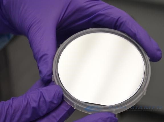
PAM-XIAMEN может предоставить эпитаксиальную пластину GaAs (арсенид галлима) со специфическим ростом для высоковольтных (HV) диодных стеков. Структура арсенида галлия обеспечивает необходимую удельную мощность, эффективность и надежность для чрезвычайно компактных систем. диодные пластины GaAs соответствуют требованиям к силовой электронике в современных промышленных приложениях, выработке электроэнергии из возобновляемых источников энергии, полностью электрическим или гибридным транспортным средствам. Особенно в диапазоне средних и высоких напряжений от 600 до 1700 вольт эпитаксиальный рост GaAs повышает энергоэффективность, а также снижает вес, размер и общую стоимость соответствующей полной системы. Ниже приведены характеристики эпитаксии GaAs с необычным и очень толстым наростом:
1. Спецификация эпитаксии GaAs
| Гомоэпитаксия GaAs для высоковольтных диодов PAMP16076-ГААС | ||||
| Слой | Материал | Концентрация допинга | Толщина | Марк |
| подложка | GaAs n-легированный | 2×10¹⁸ см-3 | – | толщина не имеет значения > 250 микрон |
| Эпи 1 | GaAs n-легированный | – | 5 микрон | – |
| Эпи 2 | GaAs p-легированный | (1-3)E15 | – | – |
| Epi 3 | GaAs p-легированный | – | – | – |
Notes for GaAs homoepitaxial films:
Thickness deviation of each layer: +/-10%;
Concentration deviation of each layer: +/-30%;
Total thickness: 15um.
LPE (liquid phase epitaxy) technology solutions can make the growing process of diode structure with high efficiency, and high quality GaAs epilayers can be obtained.
2. P-Type Doping GaAs Epitaxy on GaAs Substrate
GaAs epi wafer with high p-type doping concentration is widely used in devices such as bipolar transistors. Among p-type doped GaAs semiconductor materials, Be is an ideal p-type dopant source with many advantages. Be used as a dopant source can prepare highly doped GaAs epiwafer with controllable doping concentration to meet the requirements of the device. At the same time, Be is also a typical p-type doping source in AlGaAs, InGaAs material system devices. Be used as a p-type doping source for high-concentration doping has good advantages in device applications, such as low-resistance heterojunction bipolar transistors, p-type unalloyed ohmic contacts, etc.
There are a large number of dangling bonds on the surface of GaAs, and GaAs and As oxides are easily formed when exposed to air. These oxides will form non-radiative recombination centers and reduce the luminescence properties of GaAs materials. Therefore, reducing the surface non-radiative recombination center and surface state density of GaAs materials is of great significance to improve the luminescence performance of GaAs-based devices. Sulfur passivation is an effective treatment method to improve the luminescence properties of GaAs. After the GaAs epitaxy is subjected to sulfur passivation treatment, the oxide layer on the surface is removed, and at the same time, Ga and As on the surface combine with S to form sulfide, which reduces the surface state density, improves the radiation recombination on the surface of the epitaxial growth of gallium arsenide, and improves the photoluminescence properties of epitaxy in GaAs.
3. Unstable Growth in GaAs (001) Homoepitaxy
We use atomic force and scanning tunneling microscopy to study MBE grown GaAs (001) epitaxy. When the epitaxial growth conditions favor the island nucleation, the evolution of multilayers can be found. With the thickness of GaAs epistructures increases, the features are grown in all dimensions and the inclination angle keeps at 1°. No bumps occur on surfaces grown in step flow. We surmise the features of multilayers of GaAs epitaxy depend on island nucleation and the existence of step edge barrier because of the unstable growth mode.

For more information, please contact us email at victorchan@powerwaywafer.com и powerwaymaterial@gmail.com.