Powerway Wafer предлагает III-нитридную GaN-светодиодную пластину Epi на плоском или узорчатом сапфире, как указано ниже, которое излучает синий или зеленый свет. Размер рынка светодиодов на основе GaN составляет 50 мм, 100 мм, 150 мм или 200 мм. Длина волны излучения GaN-светодиода может достигать 530 нм.
GaN высокого кристаллического качества может быть получен путем нанесения буферного слоя при низких температурах. Благодаря такому качеству GaN были обнаружены GaN p-типа, синий pn-переход / УФ-светодиоды и стимулированное излучение при комнатной температуре.

1. Specifications of GaN Blue/Green LED Epi Wafer
Пункт 1:
100-миллиметровые пластины синего эпи-слоя GaN LED на сапфире c-plane, 445-475 нм (PAM-191010-GaN-LED);
Пункт 2:
100-миллиметровые пластины зеленого эпи-слоя GaN LED на сапфире c-plane, 510-530 нм;
Элемент 3 (пластина PAM-190320-blue GaN LED):
Синий излучающий GaN на сапфировых промышленных светодиодных пластинахс максимальной выходной мощностью и полированной тыльной стороной, что предназначено для изготовления сложных полупроводниковых приборов;
2. Parameters of GaN LED Epi Wafer on Sapphire
Параметры эпи-пластины GaN LED на сапфире:
| Кассета | Нет. | вафли ID | подложка | Wd Avg | Wd Std | FWHM Avg | Размер чипа | Vf (20 мА) | IV (mcd) | IR доходность | Выход ESD (HBM 2000) |
| 3 (25шт) | 26 | CDGB01A26 | CSS (полированный) | 452.759 | 1.477 | 20.00 | 7 * 9мил | – | 156.465 | 98,22% | 96,44% |
| 27 | CDGB01A27 | CSS (полированный) | – | 0.598 | 20.00 | – | 3.11 | – | 98,22% | – | |
| 28 | CDGB01A28 | CSS (полированный) | – | 1.346 | 20.00 | 7 * 9мил | 3.11 | 156.293 | – | 96,44% | |
| 29 | CDGB01A29 | CSS (полированный) | 452.813 | 1.016 | – | 7 * 9мил | 3.11 | – | 98,22% | – | |
| 30 | CDGB01A30 | CSS (полированный) | – | 0.863 | 20.00 | 7 * 9мил | 3.11 | – | – | 96,44% | |
| 31 | CDGB01A31 | CSS (полированный) | 451.508 | – | 20.00 | – | 3.11 | 156.05 | – | 96,44% | |
| 32 | CDGB01A32 | CSS (полированный) | – | 1.077 | 20.00 | 7 * 9мил | 3.11 | 156.05 | – | 96,44% | |
| 33 | CDGB01A33 | CSS (полированный) | 450.334 | 1.141 | 20.00 | 7 * 9мил | – | – | 98,22% | 96,44% | |
| 34 | CDGB01A34 | CSS (полированный) | – | 0.797 | 20.00 | – | 3.11 | 156.066 | 98,22% | – | |
| 35 | CDGB01A35 | CSS (полированный) | – | 0.818 | 20.00 | – | 3.11 | 155.976 | – | 96,44% | |
| 36 | CDGB01A36 | CSS (полированный) | 451.113 | – | 20.00 | 7 * 9мил | – | – | 98,22% | 96,44% | |
| 37 | CDGB01A37 | CSS (полированный) | 451.331 | 1.263 | – | – | 3.11 | – | 98,22% | 96,44% | |
| 38 | CDGB01A38 | CSS (полированный) | 451.857 | 1.65 | 20.00 | 7 * 9мил | – | 155.937 | – | 96,44% | |
| 39 | CDGB01A39 | CSS (полированный) | – | – | 20.00 | 7 * 9мил | 3.11 | 155.959 | 98,22% | 96,44% | |
| 40 | CDGB01A40 | CSS (полированный) | 452.425 | 1.071 | 20.00 | 7 * 9мил | 3.11 | – | 98,22% | – | |
| 41 | CDGB01A41 | CSS (полированный) | 453.066 | 1.381 | – | 7 * 9мил | – | 156.027 | – | 96,44% | |
| 42 | CDGB01A42 | CSS (полированный) | – | 0.88 | – | 7 * 9мил | 3.11 | 155.98 | – | 96,44% | |
| 43 | CDGB01A43 | CSS (полированный) | 453.176 | 1.204 | 20.00 | – | 3.11 | – | 98,22% | – | |
| 44 | CDGB01A44 | CSS (полированный) | 453.966 | – | 20.00 | 7 * 9мил | – | – | 98,22% | – | |
| 45 | CDGB01A45 | CSS (полированный) | 453.89 | 0.958 | – | 7 * 9мил | 3.11 | 155.88 | – | – | |
| 46 | CDGB01A46 | CSS (полированный) | 453.932 | – | 20.00 | 7 * 9мил | – | 155.846 | 98,22% | 96,44% | |
| 47 | CDGB01A47 | CSS (полированный) | – | 1.335 | 20.00 | 7 * 9мил | – | – | 98,22% | 96,44% | |
| 48 | CDGB01A48 | CSS (полированный) | 453.948 | 0.903 | 20.00 | – | – | – | – | 96,44% | |
| 49 | CDGB01A49 | CSS (полированный) | – | 0.923 | – | 7 * 9мил | – | – | – | – | |
| 50 | CDGB01A50 | CSS (полированный) | – | 1.304 | 20.00 | 7 * 9мил | – | – | 98,22% | – |
3. GaN LED Epi Process
Основной принцип эпитаксиального роста заключается в том, что на подложке (в основном сапфир (Al2O3) и SiC, Si), нагретой до соответствующей температуры, газообразные вещества In, Ga, Al и P переносятся на поверхность подложки контролируемым образом. . Выращивается специфическая тонкая монокристаллическая пленка. В настоящее время технология выращивания светодиодной эпитаксии в основном использует метод MOCVD.
Материалом подложки, используемым сейчас большинством компаний, является сапфир (Al203) для подложки GaN LED Epi. Хотя он имеет несоответствие характеристик 13,8% с GaN, тонкопленочный материал GaN, выращенный на сапфировой подложке, будет иметь очень высокую плотность дислокаций. Однако стоимость невысока, относительно зрелая технология и хорошая стабильность при высоких температурах.
4. FAQ for GaN LED Epi Wafer
Q1: What is the typical rms roughness of the polished sapphire backside surface?
Answer: It depends on your application.
Q2: Our application is to fabricate microLED devices using the epi-wafer and perform Laser Liftoff to release the devices for mass transfer and assembly. Could you kindly provide details of the thickness of each layer of the epi stack for both the Green and blue (such as total thickness of the epi-layer on sapphire, thickness of p-GaN, active region, n-GaN and the underlying u-GaN layer etc.)?
Answer: Yes, for laser liftoff application, it should be specific requirement on surface, for more information, please consult our engineer team: tech@powerwaywafer.com.
Q3: 1. These new wafers are 2 inch blue LED wafers on sapphire substrates?
2. Эти новые пластины отожжены (активированы) и отполированы с обратной стороны, так что я могу использовать их сразу же?
3. Характеристики этих новых светодиодных пластин (особенно выходная мощность) такие же или даже лучше по сравнению с пластинами, которые я купил в прошлый раз?
Answer: You requirement is: backside polished; annealed; for high power; if so, we recommend you new wafers, but it is 4”size: wavelength:475+/-5nm.
Q4: We need blue LED wafer for laser lift off(LLO) process.
If you have suitable specification wafer, we would like to get samples.
Could you give us information of spec.?
And if you have LLO experience, could you give us information?
Answer: We have some clients requesting LED wafer for laser lift off for micro LED application. For LLO, the wafers needs backside polished, which is some difficult, as during the process, it would be risky for scratch the surface.
There are two options:
Option1: LED wafer on flat sapphire, back side polished.
Option2: LED wafer on patterned sapphire, back side polished.
Q5: Do you think you could let us know if the p-GaN activation was done with in-situ anneal or ex-situ RTA process ?
Answer: We have already done a simple annealing when Mocvd is growing. This is what you call in-situ annealing, but the time is not long enough. So the chip will assist in annealing. Now all the chip processes are like this. My epitaxial wafer can go through the normal chip program.
I don’t know if the in-situ rta program you are referring to is annealed at the end of the chip with an annealing furnace. If so, then my LED/PSS epitaxial wafer does not go through this annealing.
Q6:Could you also give me some information for 4″ blue GaN LED wafers related to:
1. Current vs.output power curve;
2. Light emission spectrum of your product?
Answer: The current vs.output power curve and light emission spectrum of our blue GaN LED epi wafer are shown as figures 1 & 2, which are part of the complete data. For more comprehensive data please contact the sales team victorchan@powerwaywafer.com .(190809)
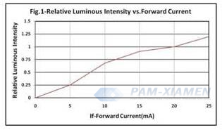
Fig.1 Characteristic Curve of Blue GaN LED Epi Wafer
Fig.2 Light Emission Spectrum of Blue GaN LED Wafer
Q7: Do you have any IQE data (IQE is a measurement of optical performance of LED stack ) about your LED epistack, is it possible to get this IQE data, do we have to pay additional fees to get them?
Anwser: The general test method is normal temperature PL test, and calculate the ratio calculation efficiency. IQE method is usually used by scientific research institutes or research institutes, there will be an additional charge, this is mainly because to test in liquid nitrogen environment, the environment is relatively special.

Для получения дополнительной информации, пожалуйста, свяжитесь с нами по электронной почте по адресу victorchan@powerwaywafer.com и powerwaymaterial@gmail.com.