We are an expert of semiconductor wafers in semiconductor industry, and we offer technology support and wafers selling for thousands of univerisities and industrial customers by our decades experience, including Cornell University, Stanford Univeristy,Peking University, Shandong Univerity, university of south carolina,Caltech Faraon lab (USA),University of California, Irvine (USA),Singapore MIT Alliance for Research and Technology Centre (SMART),West Virginia University,Purdue Univerity, University of California, Los Angeles,King Abdullah University of Science & Technology,Massachusetts Institute of Technology,University of Houston,University of Wisconsin,University of Science and Technology of China etc.
And now we show one article example as follows, who bought our wafers or service:
Article title:
Non-destructive evaluation of the strain distribution in selected-area He+ ion irradiated 4H-SiC
Published by:
Subing Yang;Sakiko Tokunaga;Minako Kondo;Yuki Nakagawa;Tamaki Shibayama;
a Graduate School of Engineering, Hokkaido University, Sapporo, Hokkaido 060-8628, Japan
b Faculty of Engineering, Hokkaido University, Sapporo, Hokkaido 060-8628, Japan
Picture of SIC Wafer:
Abstract
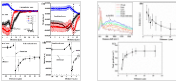
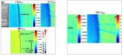
Residual strain in silicon carbide (SiC) greatly affects its physical and chemical properties and thus the performance of SiC-based devices. Herein, the detailed strain distribution in selected-area He+ ion-irradiated 4H-SiC was evaluated using the non-destructive techniques of electron backscattering diffraction and confocal Raman microscopy (CRM). In addition to the strain introduced in the irradiated area, excessive strain induced by irradiation-induced swelling also extended into the surrounding substrate. Furthermore, great compressive strain was concentrated around the interface between the irradiated and unirradiated areas. In the strain-introduced substrate, an A1(LO)/A1(LOPC) peak variation was detected by CRM, suggesting a variation of the carrier density.
Subject(s): ImplantationElectron backscattering diffraction (EBSD)Raman spectroscopyResidual strain
Article abstract for Using Wafer from Xiamen Powerway Advanced Material Co. Ltd. (PAM-XIAMEN) or Powerway Wafer Co.,Limited
“… 2. Experimental procedure. Herein, an n-type 4H-SiC (0001) single-crystal substrate
(Xiamen Powerway Advanced Material Co., Ltd, Xiamen, China) about 10 × 10 ×
0.33 mm 3 was used. This substrate was irradiated with 100 …”
Source:
https://www.sciencedirect.com/science/article/pii/S0169433219328673#!
About Xiamen Powerway Advanced Material Co., Ltd
PAM-XIAMEN offers semiconductor silicon carbide wafers,6H SiC and 4H SiC wafer in different quality grades for researcher and industry manufacturers. We has developed SiC crystal growth technology and SiC wafer processing technology. We provide custom thin film (silicon carbide)SiC epitaxy on 6H or 4H substrates for the development of silicon carbide devices. SiC epi wafer is mainly used for Schottky diodes, metal-oxide semiconductor field-effect transistors, junction field effect.
PAM-XIAMEN also offer GaAs/InP and GaN material from wafer substrate to epitaxial growth.
Powerway Wafer Co.,Limited is a sub company of Xiamen Powerway Advanced Material Co., Ltd specialize in dealing with overseas orders.
Are You Looking for an Semiconductor wafer?
PAM-XIAMEN is proud to offer semiconductor wafer inlcuidng SiC/GaN/GaAs/InP wafer with wafer or epitaxial wafer for all different kinds of projects. If you are looking for semiconductor wafer, send us enquiry today to learn more about how we can work with you to get you the substrate wafers you need for your next project. Our group team is looking forward to providing both quality products and excellent service for you! For more information, please visit our website:www.powerwaywafer.com, send us email at tech@powerwaywafer.com orpowerwaymaterial@gmail.com.