PAM XIAMEN предлагает нитрид PECVD
Нитрид PECVD является альтернативой нитриду LPCVD, когда требуются более низкие диапазоны температур. Нитрид PECVD, широко используемый в микроэлектромеханических системах (МЭМС) и обработке полупроводников, представляет собой пленку, воспринимающую напряжение при растяжении, которую можно использовать в качестве пассивирующего слоя или для балансировки напряжения пленки внутри пакета. Нитрид PECVD снижает общее напряжение пленки. Это предотвращает расслоение и микротрещины.
Также доступна услуга по более толстой пленке PECVD Niride с низким уровнем стресса.
PECVD осаждение
Стандартный оксид
Оксид медленного осаждения
OxyNitride с индивидуальным показателем преломления
Стандартный нитрид
Нитрид с низким напряжением
О PECVD
Плазменное химическое осаждение из паровой фазы (PECVD) — это метод эпитаксии при химическом осаждении из паровой фазы с возбуждением газа для создания низкотемпературной плазмы для повышения химической активности реактивных частиц. Этот метод может образовывать твердые пленки при более низких температурах. Система LPCVD показана на рисунке ниже:
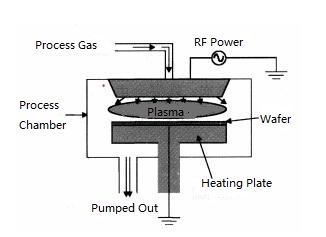
Структура реакции PECVD
For example, the matrix material is placed on the cathode in a reaction chamber, the reaction gas is fed to a lower pressure (1-600Pa), and the matrix is kept at a certain temperature. A glow discharge is generated in a certain way, the gas near the surface of the substrate is ionized, and the reactive gas is activated. At the same time, cathode sputtering occurs on the surface of the substrate, thereby improving the surface activity. There are not only the usual thermochemical reactions on the surface, but also complex plasma chemical reactions. The deposited film is formed under the combined action of these two chemical reactions. The methods of exciting glow discharge mainly include: radio frequency excitation, DC high voltage excitation, pulse excitation and microwave excitation.
The main advantages of plasma-enhanced chemical vapor deposition are that the deposition temperature is low, and the impact on the structure and physical properties of the substrate is small; the film thickness and composition uniformity are good; the film structure is dense, with few pinholes.
Films such as silicon dioxide can be deposited by PECVD on metal interconnect layers with lower melting points. In addition, PECVD has a faster deposition rate and better step coverage. It can deposit most mainstream dielectric films, including some advanced low-k materials, hard mask etc.

Для получения дополнительной информации, пожалуйста, свяжитесь с нами по электронной почте по адресуvictorchan@powerwaywafer.com и powerwaymaterial@gmail.com.