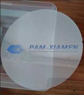
High-quality sapphire wafers are available from 2 inch to 8 inch with A, C, M or R plane. Monocrystal sapphire wafer is a very difficult material to process, so it is often used as a material for optoelectronic components. At present, the quality of ultra-high-brightness white/blue LEDs depends on the material quality of gallium nitride epitaxy (GaN), and the quality of LED GaN epitaxy is closely related to the surface processing quality of the sapphire substrate wafer. The lattice constant mismatch rate between C-plane sapphire and the II-V and II-VI group deposited films is small, and it meets the high temperature resistance requirements in the GaN epitaxial process, making the sapphire wafer a key material for the production of white/blue/green LEDs. As one of sapphire wafer suppliers, PAM-XIAMEN offers you following sapphire wafer specifications:
2 сапфира WAFER A-САМОЛЁТА 11-20 МОНОКРИСТАЛЛ al2o3
Материал: высокая чистота> 99,996%, монокристалл Al2O3
Dimension: Φ50.8 mm ± 0.1 mm
Thickness: 0.50 mm standard
Lattice Parameter: a=4.785 A, c=12.991 A
Density: 3.98 g/cm3
Orientation: A-plane (11-20) 0.2± 0.1 degree off.
Primary Flat Orientation: C-plane
Primary flat length: 16.0 ± 1 mm
Total Thickness Variation: <10 μm
Bow: <10 μm
Warp: <10 μm
Polishing: single side polished Ra < 0.5 nm (AFM), double size polish is available per request.
2 сапфира WAFER M-САМОЛЁТА 10-10 МОНОКРИСТАЛЛ al2o3
Материал: высокая чистота> 99,996%, монокристалл Al2O3
Dimension: Φ50.8 mm ± 0.1 mm
Thickness: 0.43 mm standard
Lattice Parameter: a=4.785 A, c=12.991 A
Density: 3.98 g/cm3
Orientation: M-plane (10-10) 0.2± 0.1 degree off.
Primary flat orientation: C-plane[11-20] +/- 0.2°
Primary flat length: 16.0 ± 1 mm
Total Thickness Variation: <10 μm
Bow: <10 μm
Warp: <10 μm
Polishing: single side polished Ra < 0.5 nm (AFM), double size polish is available per request.
2 сапфира WAFER R-САМОЛЁТА 1-102 МОНОКРИСТАЛЛ al2o3
Материал: высокая чистота> 99,996%, монокристалл Al2O3
Dimension: Φ50.8 mm ± 0.1 mm
Thickness: 0.43 mm standard
Lattice Parameter: a=4.785 A, c=12.991 A
Density: 3.98 g/cm3
Orientation: R-plane (1-102) 0.2± 0.1 degree off.
Primary Flat orientation: Projected C-Axis 45 +/- 2 degree
Primary flat length: 16.0 ± 1 mm
Total Thickness Variation: <10 μm
Bow: <10 μm
Warp: <10 μm
Polishing: single side polished Ra < 0.5 nm (AFM), double size polish is available per request.
2 ДЮЙМОВЫЕ САПФИРА ВАФЛЯ С-САМОЛЕТ одной или двух сторон ПОЛЬСКО AL2O3 МОНОКРИСТАЛЛ
Материал: высокая чистота> 99,99%, монокристалл Al2O3
Dimension: Φ50.8 mm ± 0.1 mm
Thickness: 430 um ± 25 um for SSP and 400 um ± 25 um for DSP (other thickness available upon request)
Lattice Parameter: a=4.785 A, c=12.991 A
Density: 3.98 g/cm3
Orientation: C plane (0001) to M (1-100) 0.2 ± 0.1 degree off.
Primary Flat Orientation: A-plane [11-20] +/- 0.2°
Primary Flat Length: 16.0 ± 1.0 mm
Total Thickness Variation (TTV): <5 μm
Bow: <10 μm
Warp: <10 μm
Polishing: single side polished (SSP) front side epi-ready surface Ra < 0.3 nm (AFM), back side fine-ground Ra = 0.8 ~ 1.2 um, or double side polished (DSP) both front and back sides epi-ready surface Ra < 0.3 nm (AFM)
3 ДЮЙМОВЫЕ САПФИРА ВАФЛЯ С-САМОЛЕТ одной или двух сторон ПОЛЬСКО AL2O3 МОНОКРИСТАЛЛ
Материал: высокая чистота> 99,99% монокристалл Al2O3
Diameter: Φ76.2 mm ± 0.1 mm
Thickness: 650 um ± 25 um (SSP) , 600 or 430 um ± 25 um (DSP)
Lattice Parameter: a=4.785 A, c=12.991 A
Density: 3.98 g/cm3
Orientation: C plane (0001) ± 0.3 degree, R-plane (1-102), A-plane (11-20), M-plane (10-10) are available.
Primary flat orientation: A-plane ± 0.3 degree
Primary flat length: 22.0 mm ± 1 mm
Total Thickness Variation (TTV): <15 μm
Bow: <15 μm
Warp: <15 μm
Polishing: single side polished (SSP) front side epi-ready surface Ra < 0.5 nm (AFM), back side fine-ground Ra = 0.8 ~ 1.2 um, or double side polished (DSP) both front and back sides epi-ready surface Ra < 0.5 nm (AFM)
4 ДЮЙМОВЫЕ САПФИРА ВАФЛЯ С-САМОЛЕТ одной или двух сторон ПОЛЬСКО AL2O3 МОНОКРИСТАЛЛ
Материал: высокая чистота,> 99,99%, монокристалл Al2O3
Dimension: Φ100.0 mm ± 0.1 mm
Thickness: 650 um ± 25 um (SSP) , 600 um ± 25 um (DSP)
Lattice Parameter: a=4.785 A, c=12.991 A
Density: 3.98 g/cm3
Orientation: C plane sapphire (0001) off M plane 0.2± 0.1 degree, R-plane (1-102), A-plane (11-20), M-plane (10-10) are available.
Primary flat orientation: A-plane ± 0.2 degree
Primary flat length: 30.0 ± 1 mm
Total Thickness Variation (TTV): <20 μm
Bow: <20 μm
Warp: <20 μm
Polishing: single side polished (SSP) front side epi-ready surface Ra < 0.5 nm (AFM), back side fine-ground Ra = 0.8 ~ 1.2 um, or double side polished (DSP) both front and back sides epi-ready surface Ra < 0.5 nm (AFM)
6 inch C-plane (0001) Sapphire Substrate (PAM210910-S)
| Item | Specification |
| Material | High Purity Al2O3 |
| Growth Method | KY |
| Surface Orientation | C-plane (0001) off Angle 0.2°±0.1°(M-axis); 0°±0.1°(A-axis) |
| Diameter | 150±0.2mm |
| Thickness | 1300±25um |
| TTV | ≤15um |
| Bow | -20~0um |
| Warp | ≤25um |
| Wafer Edge | T-type or R-type |
| R-plane | R9 |
| Primary Flat Orientation | A-plane±0.2° |
| Primary Flat Length | Semi-notch/47.5±1.5mm |
| Front Surface Roughness | Ra≤0.3nm |
| Back Surface Roughness | 0.8~1.2um |
| Laser Mark | Back or Front Side (Backside Preferred) |
| Package | 25pcs/cassette, vacuum-sealed, nitrogen-filled, class-100 cleanroom |
Sapphire Wafer 200mm (PAM210910-S)
| Item | Specification |
| Material | High Purity Al2O3 |
| Surface Orientation | C-plane (0001) off Angle 0°±0.3°(M-axis) |
| Diameter | 200±0.25mm |
| Thickness | 725±25um |
| TTV | ≤20um |
| Bow | -30~0um |
| Warp | ≤25um |
| Wafer Edge | T-type or R-type |
| R-plane | R9 or R3 |
| Primary Flat Orientation | A-plane±0.2° |
| Primary Flat Length | Semi-notch/Design by customer |
| Front Surface Roughness | Ra≤0.3nm |
| Back Surface Roughness | 0.8~1.2um |
| Laser Mark | Back or Front Side (Backside Preferred) |
| Package | 25pcs/cassette, vacuum-sealed, nitrogen-filled, class-100 cleanroom |
R-Plane Sapphire Substrate with SSP

For more information, please contact us email at victorchan@powerwaywafer.com и powerwaymaterial@gmail.com.